High pressure rf-dc sputtering and methods to improve film uniformity and step-coverage of this process

a technology of rf-dc sputtering and high pressure, which is applied in the direction of vacuum evaporation coating, electrolysis components, coatings, etc., can solve the problems of increasing the risk of contamination, unfavorable interfacial layer, and increasing the detrimental effect of interfacial layer or contamination formation, so as to reduce the productivity of field effect transistor manufacturing

Inactive Publication Date: 2010-10-07
APPLIED MATERIALS INC
View PDF19 Cites 83 Cited by
  • Summary
  • Abstract
  • Description
  • Claims
  • Application Information

AI Technical Summary

Benefits of technology

[0011]In one embodiment of the invention, a high pressure RF DC PVD chamber is disclosed having a dual ring magnetron comprising asymmetric magnet rings, a low profile cover ring and deposition ring, and a pedestal capacitive tuner.
[0012]In another embodiment of the invention, a method for depositing a metal film is disclosed. The method includes flowing a high pressure gas into a chamber, igniting a plasma from the gas using an RF and DC power source electrically connected to a sputtering target, forming a dense plasma by using a magnetron, tuning a pedestal to match the RF power source, and depositing a metal film on a substrate in the chamber.

Problems solved by technology

In the ambient environment, the substrates are exposed to mechanical and chemical contaminants, such as particles, moisture, and the like, that may damage the gate structures being fabricated and possibly form an undesired interfacial layer, e.g., native oxide, between each layer while transferring.
As gate structures become smaller and / or thinner to increase the device speed, the detrimental effect of forming interfacial layers or contamination becomes an increased concern.
Additionally, the time spent on transferring the substrate between the cluster tools decreases productivity in manufacture of the field effect transistors.
However, residual particles from organo-metallic precursors may contaminate the underlying dielectric layers when forming the metal portion of the gate stack, adversely affecting the dielectric properties of the gate dielectric layer.
Furthermore, as transistor sizes decrease below 45 nm and have higher aspect ratios, achieving sufficient film uniformity and step-coverage becomes increasingly difficult.

Method used


Image

  • High pressure rf-dc sputtering and methods to improve film uniformity and step-coverage of this process
  • High pressure rf-dc sputtering and methods to improve film uniformity and step-coverage of this process
  • High pressure rf-dc sputtering and methods to improve film uniformity and step-coverage of this process

Examples


Embodiment Construction

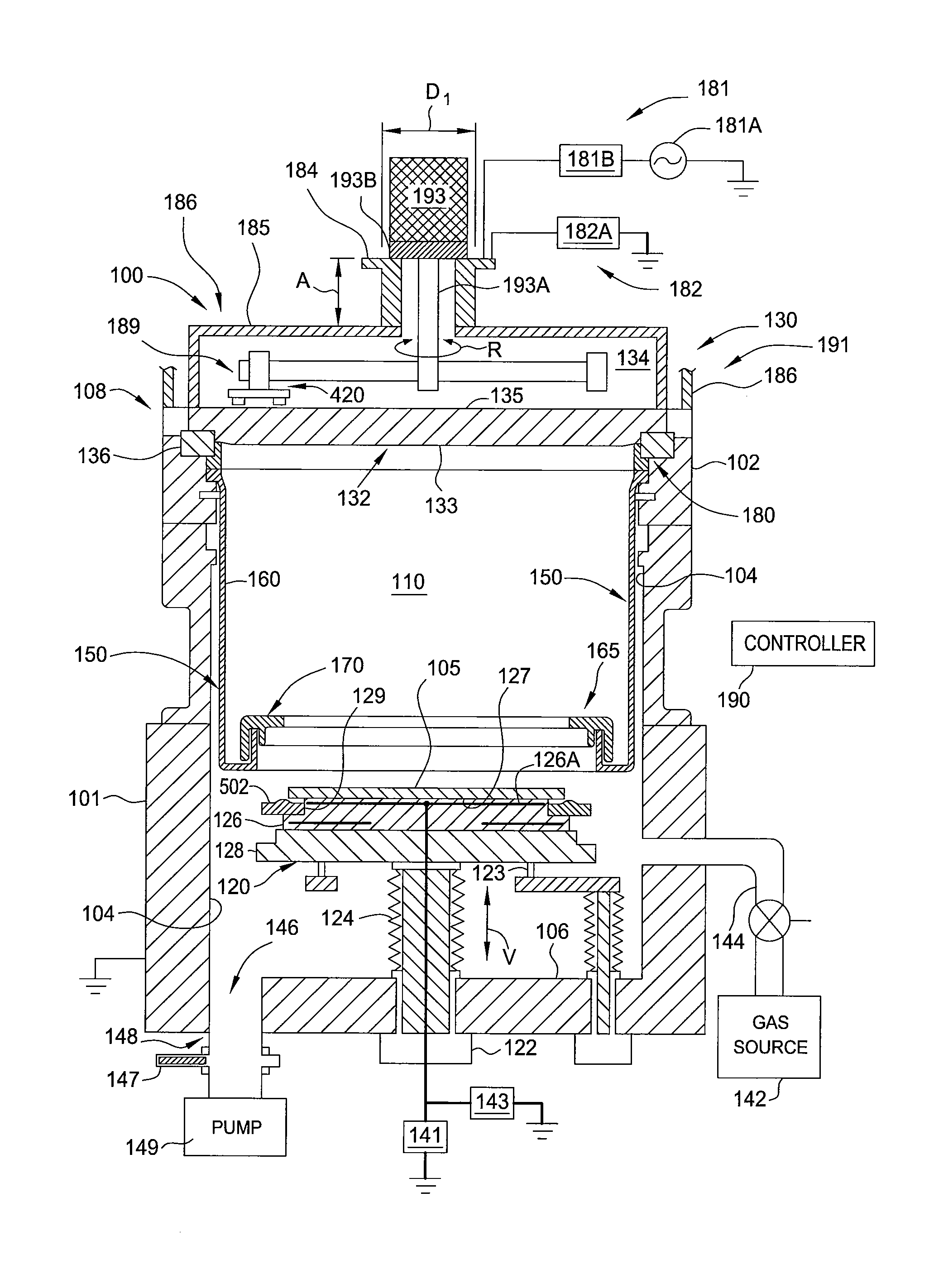
[0034]Embodiments of the invention generally provide a processing chamber used to perform a physical vapor deposition (PVD) process. In one embodiment, the process chamber design is adapted to deposit a desired material using an RF physical vapor deposition (PVD) process. The processing chamber disclosed herein may be especially useful for depositing multi-compositional films. The processing chamber's design features may include: an improved RF feed configuration to reduce any standing wave effects; an improved magnetron design to enhance RF plasma uniformity, deposited film composition and thickness uniformity; an improved substrate biasing configuration to improve process control; and an improved process kit design to improve RF field uniformity near the critical surfaces of the substrate to promote greater process uniformity and repeatability.

[0035]FIG. 1A illustrates an exemplary semiconductor processing chamber 100 having an upper process assembly 108, a process kit 150 and a p...


PUM

PropertyMeasurementUnit
dielectric constantaaaaaaaaaa
sizesaaaaaaaaaa
frequencyaaaaaaaaaa

Abstract

Embodiments of the invention generally provide a processing chamber used to perform a physical vapor deposition (PVD) process and methods of depositing multi-compositional films. The processing chamber may include: an improved RF feed configuration to reduce any standing wave effects; an improved magnetron design to enhance RF plasma uniformity, deposited film composition and thickness uniformity; an improved substrate biasing configuration to improve process control; and an improved process kit design to improve RF field uniformity near the critical surfaces of the substrate. The method includes forming a plasma in a processing region of a chamber using an RF supply coupled to a multi-compositional target, translating a magnetron relative to the multi-compositional target, wherein the magnetron is positioned in a first position relative to a center point of the multi-compositional target while the magnetron is translating and the plasma is formed, and depositing a multi-compositional film on a substrate in the chamber.

Description

CROSS-REFERENCE TO RELATED APPLICATIONS[0001]This application claims benefit of U.S. Provisional Patent Application Ser. No. 61 / 166,682 (APPM / 014067L), filed Apr. 3, 2009, which is herein incorporated by reference. This application also claims benefit of U.S. Provisional Patent Application Ser. No. 61 / 319,377 (APPM / 015091 L), filed Mar. 31, 2010, which is herein incorporated by reference.BACKGROUND OF THE INVENTION[0002]Embodiments of the present invention generally relate to methods and an apparatus of forming metal and dielectric layers. More particularly, embodiments of the invention relate to methods and an apparatus for forming a metal gate and associated dielectric layers.DESCRIPTION OF THE RELATED ART[0003]Integrated circuits may include more than one million micro-electronic devices such as transistors, capacitors, and resistors. One type of integrated circuit are field effect transistors (e.g., complementary metal-oxide-semiconductor (CMOS) field effect transistors) that ar...

Claims


Application Information

Patent Timeline
Patent Type & Authority Applications(United States)
IPC IPC(8): C23C14/34
CPCC23C14/345C23C14/35C23C14/548H01J37/3455H01J37/32642H01J37/3408H01J37/3441C23C14/564H01J37/3405C23C14/34H01L21/02H01L21/02266H01L21/02521H01L21/02631H01L21/203H01L21/2855H01L21/324H01J37/345H01J37/3452H01J37/3411C23C14/3492
Inventor ALLEN, ADOLPH MILLERHAWRYLCHAK, LARAXIE, ZHIGANGRASHEED, MUHAMMAD M.WANG, RONGJUNTANG, XIANMINLIU, ZHENDONGGUNG, TZA-JINGGANDIKOTA, SRINIVASCHANG, MEICOX, MICHAEL S.YOUNG, DONNYSAVANDAIAH, KIRANKUMARGE, ZHENBIN
Owner APPLIED MATERIALS INC
Why Eureka
Try Eureka