
Scanning electron microscope with measurement function

a scanning electron microscope and function technology, applied in the direction of instruments, semiconductor/solid-state device testing/measurement, nuclear engineering, etc., can solve the problems of difficult to check, troublesome to revise and check stored amp data, etc., and achieve the effect of efficient and easy measuremen

Inactive Publication Date: 2006-10-05
OJIMA YUUKI +3
View PDF15 Cites 0 Cited by
  • Summary
  • Abstract
  • Description
  • Claims
  • Application Information

AI Technical Summary

Benefits of technology

"The present invention provides a scanning electron microscope that can efficiently and easily make measurements for multiple items. It also allows for easy storage, checking, and revision of automatic measurement parameters. The microscope can create line profiles from SEM images and detect edges using various methods. The measurements can then be calculated based on the specified parameters. This invention simplifies the process of making multiple measurements and improves the efficiency of the scanning electron microscope."

Problems solved by technology

Therefore, in semi-auto measurement, if several types of measurements are to be made, it is necessary to specify a set of AMP for each measurement type, which is very troublesome.
In full-auto measurement, if several types of measurements are to be made, required AMP data is stored in a recipe file and thus operation is easy, but it is troublesome to revise and check the stored AMP data.
A resulting measurement value is displayed in a window of the SEM upon execution of measurement; when several types of measurements are made, it is not easy to check numerical measurement values so the operator has to wait for completion of the whole measurement process until a list of measurement results appears.

Method used


Image

  • Scanning electron microscope with measurement function
  • Scanning electron microscope with measurement function
  • Scanning electron microscope with measurement function

Examples


Embodiment Construction

[0035] Next, preferred embodiments of the present invention will be described referring to the accompanying drawings.

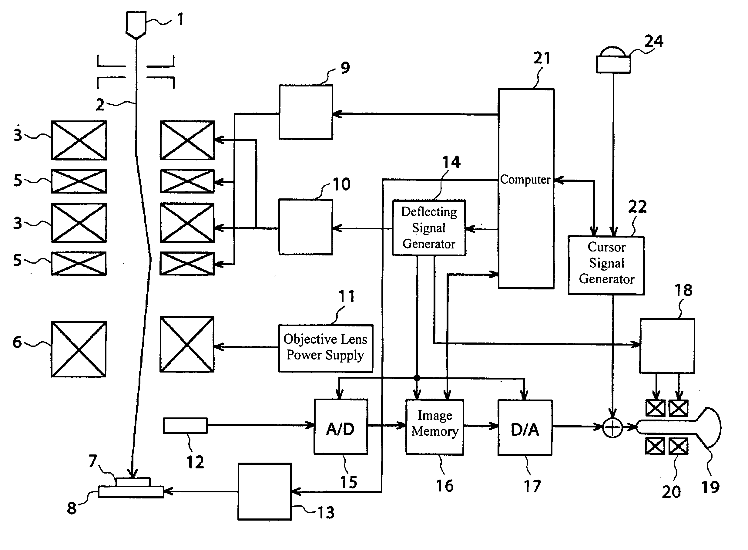
[0036]FIG. 15 shows the general structure of a scanning electron microscope with a measurement function according to an embodiment of the present invention (see Patent Document 1). An electron beam 2 emitted from an electron gun 1 is narrowed by an objective lens 6 and thrown on a sample 7. The objective lens 6 is excited by an objective lens power supply 11. A deflecting signal generator 14 sends a deflecting signal depending on a scanning area or scanning position of the electron beam 2 as indicated by a computer 21 through a deflecting amplifier 10 to a deflecting coil 5 to excite it so that the sample 7 is scanned with the electron beam 2 two-dimensionally.

[0037] A secondary signal (secondary electron signal, reflection electron signal, etc.), which is generated from the sample 7 in response to irradiation of the electron beam 2, is detected by a detector 12 and...


PUM

PropertyMeasurementUnit
distanceaaaaaaaaaa
Thresholdaaaaaaaaaa
scanning electron microscopeaaaaaaaaaa

Abstract

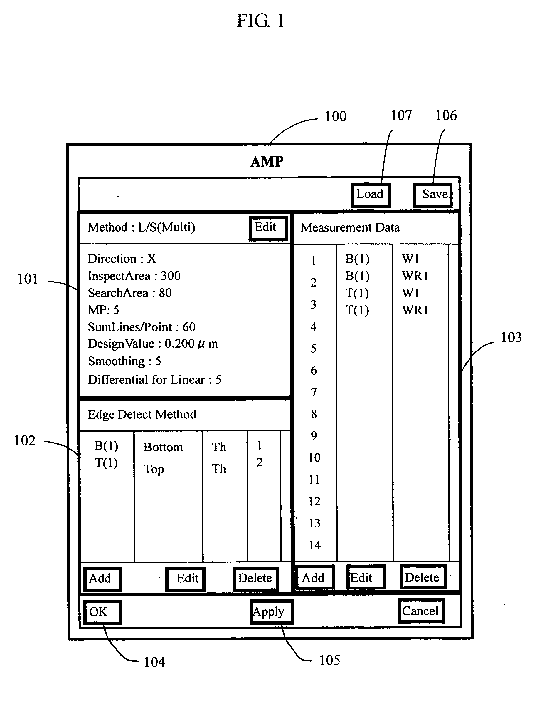
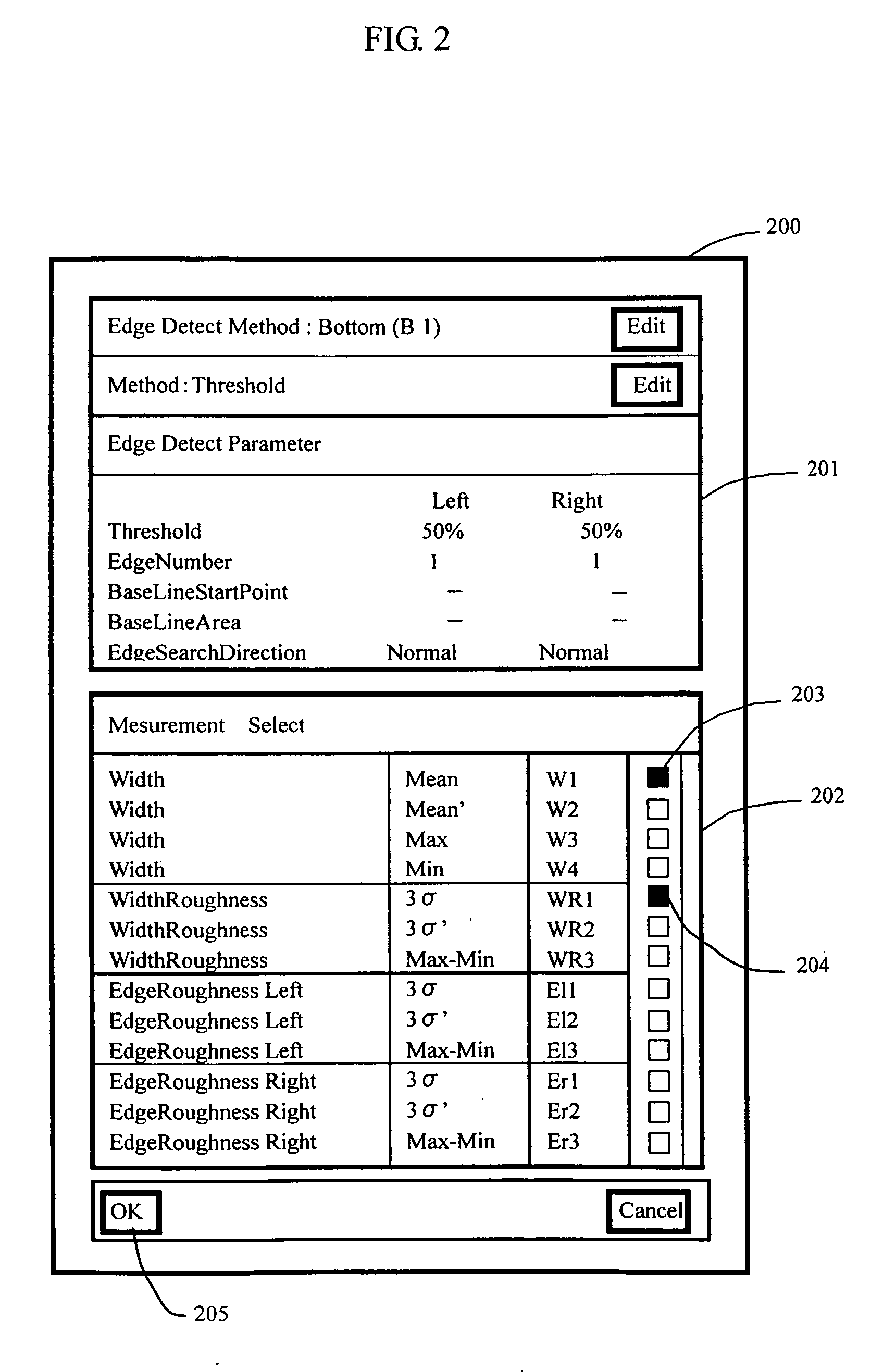
A scanning electron microscope which efficiently makes measurements for plural measurement items at a time and allows easy entry, confirmation and revision of auto measurement parameters. Parameters for creation of a line profile from an image captured by the scanning electron microscope are entered as auto measurement parameters (AMP) to be used as common conditions for all measurement items. Also, plural combinations of edge detection methods and measurement calculation methods are entered as auto measurement parameters to make measurements for plural items.

Description

FIELD OF THE INVENTION [0001] The present invention relates to a scanning electron microscope with a measurement function and a measurement method which uses it. BACKGROUND OF THE INVENTION [0002] The following patent documents (gazettes) describe conventional techniques in this field: [0003] Patent Document 1: JP-A No. 347246 / 1994 [0004] Patent Document 2: JP-A No. 22794 / 1996 [0005] Patent Document 3: JP-A No. 237231 / 1999 [0006] Patent Document 4: JP-A No. 213427 / 1998 [0007] Patent Document 5: JP-A No. 201919 / 1999 [0008] A scanning electron microscope with a measurement function (hereinafter called a measurement SEM) has been used for control of semiconductor sample dimensions or other similar purposes. There are two dimensional measurement modes: a manual measurement mode and an auto measurement mode. In the manual measurement mode, an operator visually makes a measurement using a measurement cursor. In the auto measurement mode, a measurement SEM captures an image of a pattern to...

Claims


Application Information

Patent Timeline
Patent Type & Authority Applications(United States)
IPC IPC(8): G21K7/00G01N23/00G01B15/00G01N23/225H01J37/22H01J37/28H01L21/66
CPCG01N23/2251H01J37/265H01J2237/2817H01J2237/221H01J2237/2816H01J37/28
Inventor OJIMA, YUUKISASADA, KATSUHIROUEDA, KAZUHIROMORIMOTO, TSUYOSHI
Owner OJIMA YUUKI
Learn More