Semiconductor light-emitting device mounting member, light-emitting diode constituting member using same, and light-emitting diode using same

a technology of semiconductors and mounting parts, which is applied in the direction of semiconductor devices, basic electric elements, electrical equipment, etc., can solve the problems of difficult formation of aluminum surface layers, and achieve the effect of eliminating the waste of costly packages

Active Publication Date: 2006-10-05
SUMITOMO ELECTRIC IND LTD
View PDF1 Cites 83 Cited by
  • Summary
  • Abstract
  • Description
  • Claims
  • Application Information

AI Technical Summary

Benefits of technology

[0018] An object of the present invention is to offer a semiconductor-light-emitting-device-mounting member capable of eliminating the waste of a costly package, a semiconductor light-emitting device, a substrate, a fluorescent body, and so on. This capability is to be given by the ability to examine the presence or absence of a faulty property of the semiconductor light-emitting device and the shade of color of the light before the light-emitting device is incorporated into the light-emitting diode or surface light-emitting body.

Problems solved by technology

However, it is difficult to form the aluminum surface layer on the metallized layer by the plating method, which is another problem.

Method used


Image

  • Semiconductor light-emitting device mounting member, light-emitting diode constituting member using same, and light-emitting diode using same
  • Semiconductor light-emitting device mounting member, light-emitting diode constituting member using same, and light-emitting diode using same
  • Semiconductor light-emitting device mounting member, light-emitting diode constituting member using same, and light-emitting diode using same

Examples


Embodiment Construction

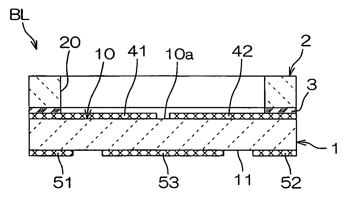
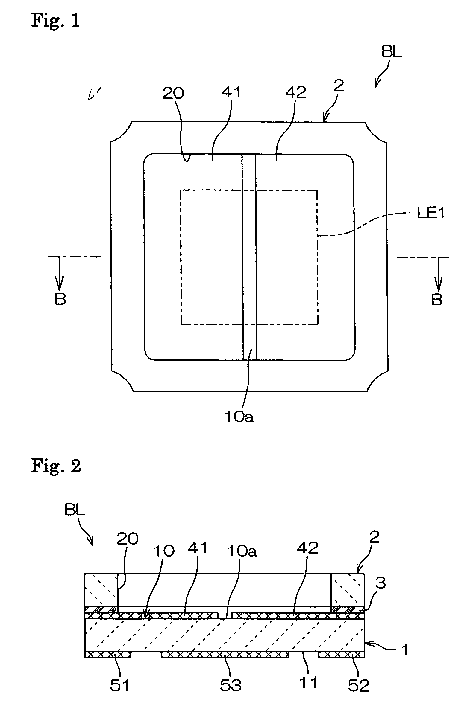
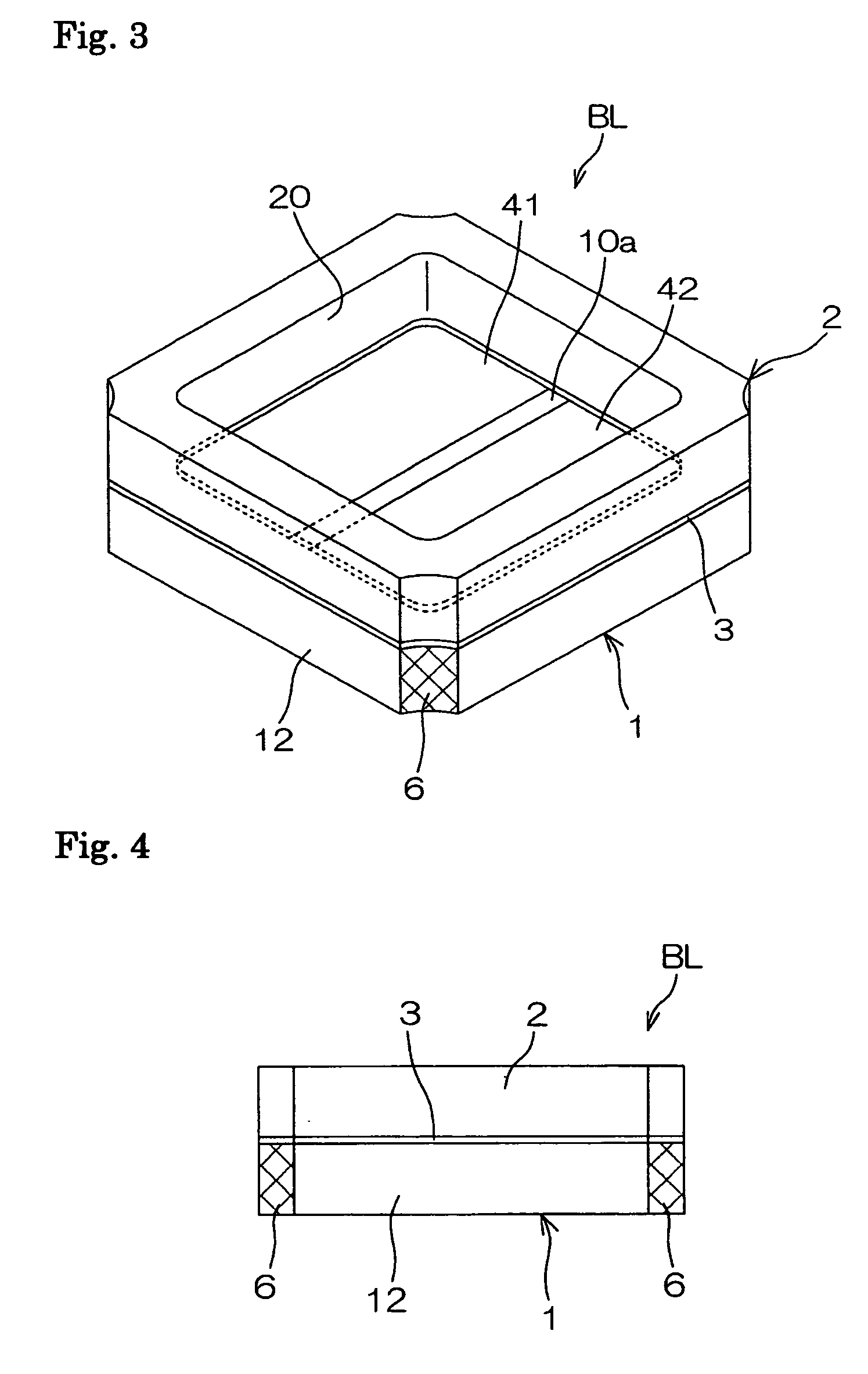
[0088]FIG. 1 is a plan view showing an example of an embodiment of a semiconductor-light-emitting-device-mounting member BL of the present invention. FIG. 2 is a view showing the cross section cut by the line B-B in FIG. 1. FIG. 3 is a perspective view showing the entire semiconductor-light-emitting-device-mounting member BL of the above-described example. FIG. 4 is a side view of it.

[0089] As can be seen from these figures, the semiconductor-light-emitting-device-mounting member BL of this example is provided with a flat-shaped highly heat-dissipative member 1 that has a nearly square shape when viewed from above and that has a main surface 10, which is the top surface in the foregoing figures. A frame-shaped member 2, whose outside wall runs along with the four sides of the square of the highly heat-dissipative member 1, is placed on the main surface 10 as a component of the member BL.

[0090] In this example, the frame-shaped member 2, which has a flat shape similar to that of th...


PUM


Abstract

A semiconductor-light-emitting-device-mounting member BL comprises (a) a highly heat-dissipative member 1 having a main surface 10 on which connecting-use electrode layers 41 and 42 are provided to form a device-mounting area 10a and (b) a frame-shaped member 2 placed on the main surface 10 so as to surround the device-mounting area 10a. The device-mounting area 10a has an area that is 1.05 to 4 times the area of a semiconductor light-emitting device LE1. A light-emitting-diode-constituting member LE2 mounts a semiconductor light-emitting device LE1 on the device-mounting area 10a of the semiconductor-light-emitting-device-mounting member BL and has a fluorescent body and / or a protective resin LR filling the inside space of the frame-shaped member 2. A light-emitting diode LE3 mounts the light-emitting-diode-constituting member LE2 on a package 7.

Description

TECHNICAL FIELD [0001] The present invention relates to a semiconductor-light-emitting-device-mounting member to be used to form a light-emitting diode by using a semiconductor light-emitting device, a light-emitting-diode-constituting member that mounts a semiconductor light-emitting device on the semiconductor-light-emitting-device-mounting member, and a light-emitting diode that mounts the light-emitting-diode-constituting member on it. BACKGROUND ART [0002] When a light-emitting diode is formed by using a chip-shaped semiconductor light-emitting device in which a light-emitting layer and an electrode layer are formed on a semiconductor substrate, it is a common practice to use a package having a recessed portion (see Literature 1: the published Japanese patent application 2002-232017). The package described in Literature 1 uses the bottom surface of the recessed portion as a mounting portion for mounting a semiconductor light-emitting device to allow light emitted from the semic...

Claims


Application Information

Patent Timeline
Patent Type & Authority Applications(United States)
IPC IPC(8): H01L33/00H01L33/50H01L33/56H01L33/58H01L33/62H01L33/64
CPCH01L33/486H01L33/62H01L33/641H01L2224/16225H01L2224/48247H01L2224/48091H01L2924/00014H01L2924/00011H01L2224/0401
Inventor HIGAKI, KENJIROISHIDU, SADAMUAMOH, TERUOTSUZUKI, YASUSHI
Owner SUMITOMO ELECTRIC IND LTD
Why Eureka
Try Eureka