Display device with built-in sensor

a display device and sensor technology, applied in the field of flat-panel display devices, can solve problems such as product malfunctions and in some cases, and achieve the effect of stable sensor outpu

Inactive Publication Date: 2006-10-05
TOSHIBA MATSUSHITA DISPLAY TECH
View PDF4 Cites 42 Cited by
  • Summary
  • Abstract
  • Description
  • Claims
  • Application Information

AI Technical Summary

Benefits of technology

[0010] An object of the embodiments of the present invention is to provide a display device with a built-in sensor, which can obtai

Problems solved by technology

For this reason, when the sensor is used as a pen-input panel or a touch panel, such produ

Method used


Image

  • Display device with built-in sensor
  • Display device with built-in sensor
  • Display device with built-in sensor

Examples


Embodiment Construction

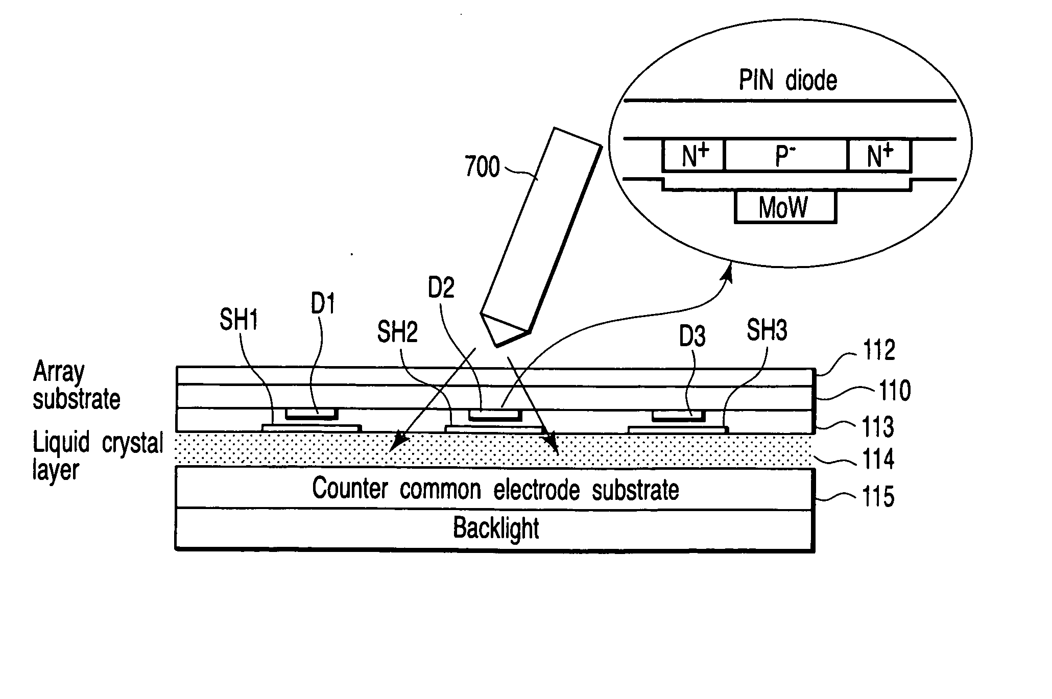
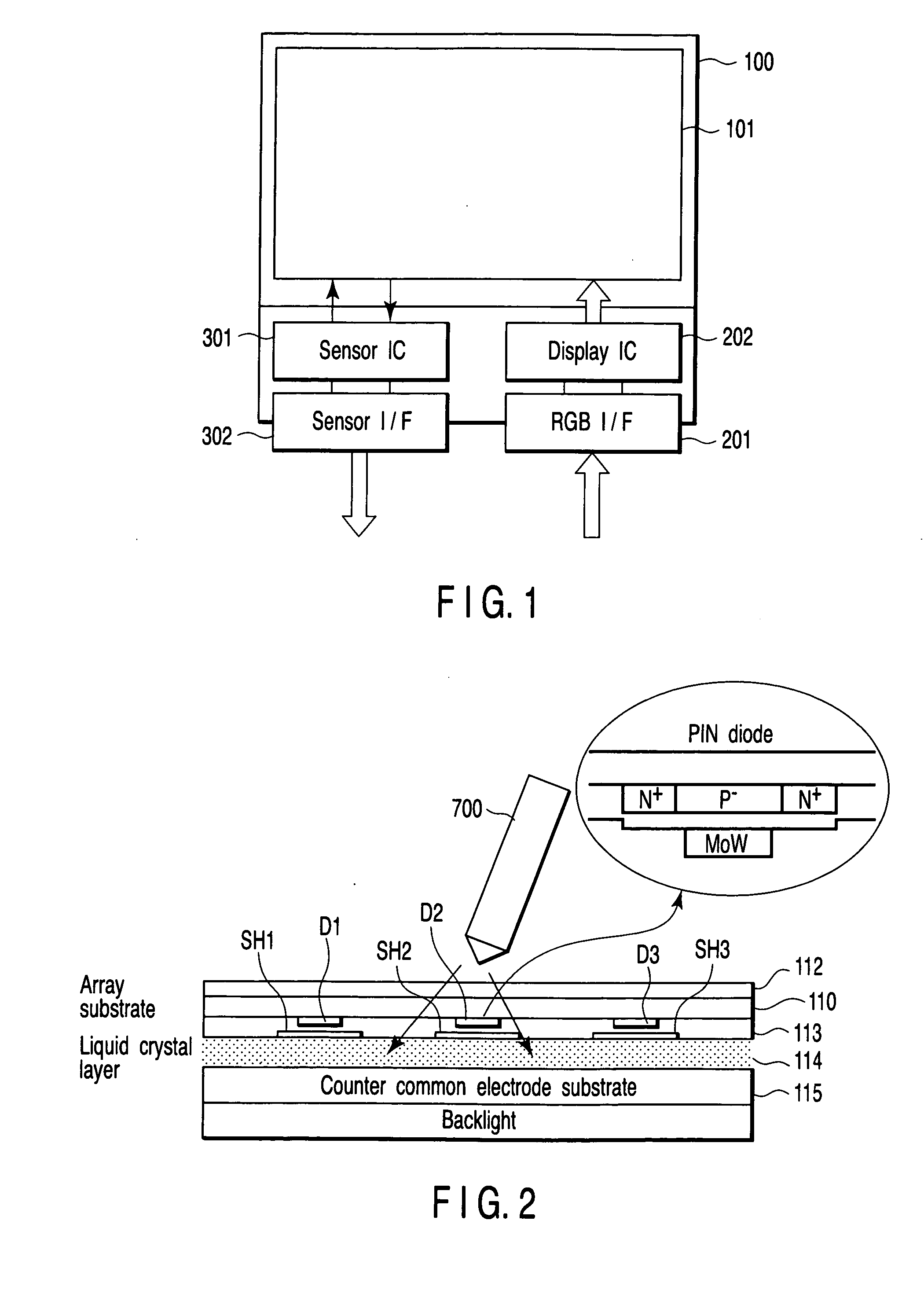
[0024] Embodiments of the present invention will now be described with reference to accompanying drawings. FIG. 1 schematically illustrates a built-in sensor type display device 100 according to the present invention. The built-in sensor type display device 100 has a display region 101 which includes a glass substrate. On a back side of the glass substrate, display pixel circuits that are arranged in a two-dimensional manner and sensor circuits that are arranged in a two-dimensional manner are arranged as will be described.

[0025] A display image signal output from an image output circuit is input to a display IC 202 via an RGB interface 201. The display IC 202 includes a signal line drive circuit, a pixel gate drive circuit, etc., and it supplies a display image signal to the display image circuit.

[0026] The sensor output image signal read from the sensor circuit is read out by the sensor IS 301, and it is guided to an image processing unit via a sensor interface 302.
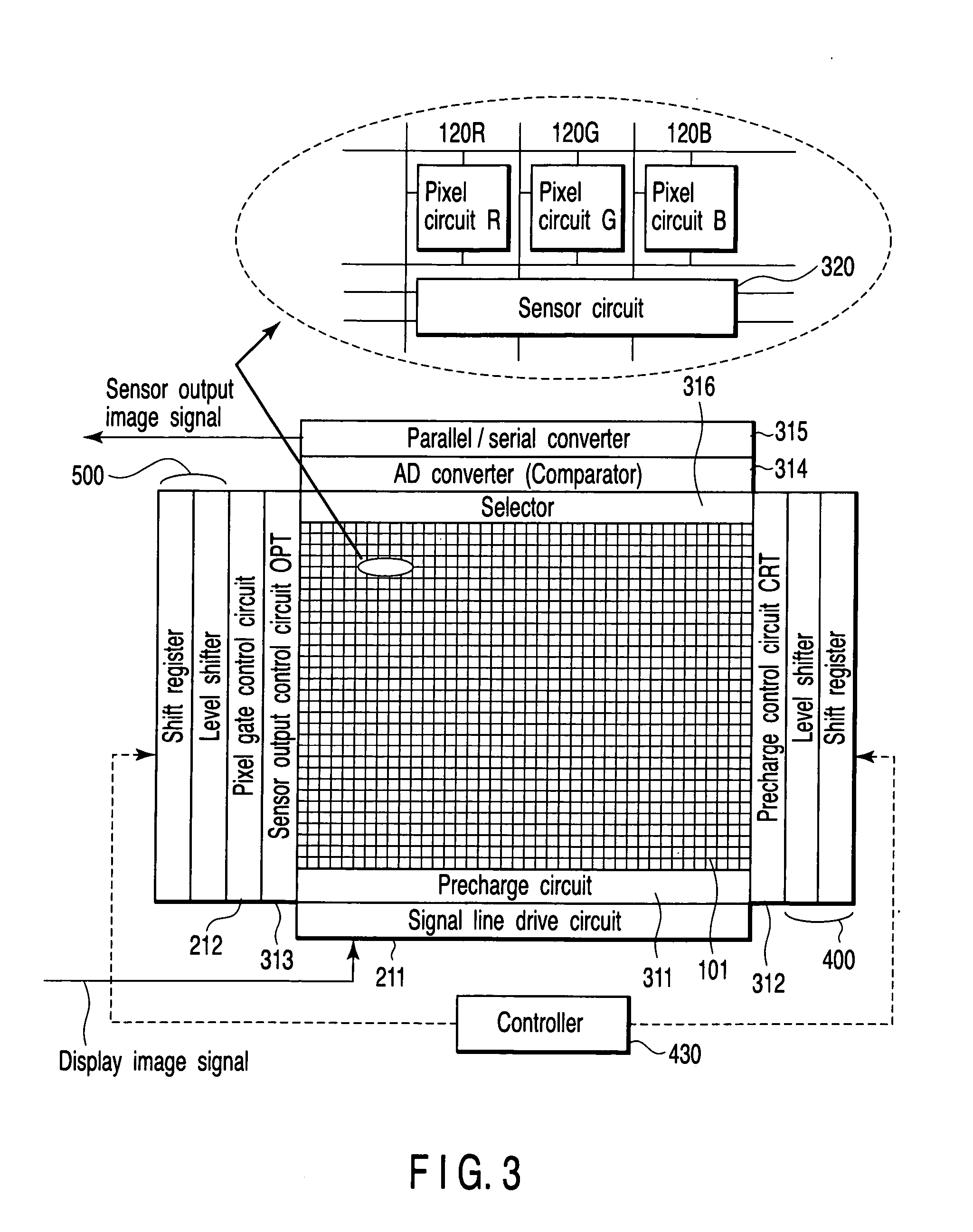
[0027]FIG. 2...


PUM


Abstract

A drive circuit that can cover a possible dispersion in characteristics among optical sensors is constructed in order to obtain a stable sensor output. The device includes an optical sensor provided in each of pixels arranged in lines in vertical and horizontal directions, a circuit that instructs a timing of precharge for the optical sensor, and a circuit that instruct a timing for outputting data of the optical sensor from a respective pixel. The device further comprises means that changes the timing for precharge and the timing for outputting the data each to an arbitrary interval.

Description

CROSS-REFERENCE TO RELATED APPLICATIONS [0001] This application is based upon and claims the benefit of priority from prior Japanese Patent Application No. 2005-060306, filed Mar. 4, 2005, the entire contents of which are incorporated herein by reference. BACKGROUND OF THE INVENTION [0002] 1. Field of the Invention [0003] The present invention relates to a flat-panel type display device that employs liquid crystal, light-emitting device and the like, and more specifically, to a sensor-equipped display device with a built-in input sensor. [0004] 2. Description of the Related Art [0005] Conventionally, liquid crystal display devices include an array substrate on which signal lines, scanning lines and pixel transistors (for example, thin film transistors: TFTs) are arranged, and a drive circuit that drives the signals lines and scanning lines. Due to the recent progress and development in the technology of the integrated circuit, a processing technique that forms a part of a drive circ...

Claims


Application Information

Patent Timeline
IPC IPC(8): H01L31/113
CPCG02F2001/13312H01L27/14601G06F3/0412G06F3/042G02F1/13312
Inventor HAYASHI, HIROTAKANAKAMURA, TAKASHI
Owner TOSHIBA MATSUSHITA DISPLAY TECH
Why Eureka
Try Eureka