Tunneling-enhanced floating gate semiconductor device

a technology of enhanced floating gate and semiconductor device, which is applied in the direction of semiconductor devices, solid-state devices, instruments, etc., can solve the problems of constant power and data loss of volatile memory, and achieve the effect of facilitating tunneling-enhanced floating gate operation

Inactive Publication Date: 2006-10-05
VIRAGE LOGIC
View PDF6 Cites 18 Cited by
  • Summary
  • Abstract
  • Description
  • Claims
  • Application Information

AI Technical Summary

Benefits of technology

[0007] The disclosure facilitates tunneling-enhanced floating gate operation in a semiconductor device. Accordingly, the disclosure provides a programming and erasing circuit for memory devices.
[0008] In some embodiments, a junction device is configured with predetermined regions of its floating gate and a surface region implanted with p+ or n+ type impurities to enhance tunneling capability. As a result higher tunneling currents may be achieved without increasing the tunneling voltage, or same tunneling currents may be achieved for lower tunneling voltage values.

Problems solved by technology

Volatile memory loses any data as soon as the system is turned off.
Thus, it requires constant power to remain viable.

Method used


Image

  • Tunneling-enhanced floating gate semiconductor device
  • Tunneling-enhanced floating gate semiconductor device
  • Tunneling-enhanced floating gate semiconductor device

Examples


Embodiment Construction

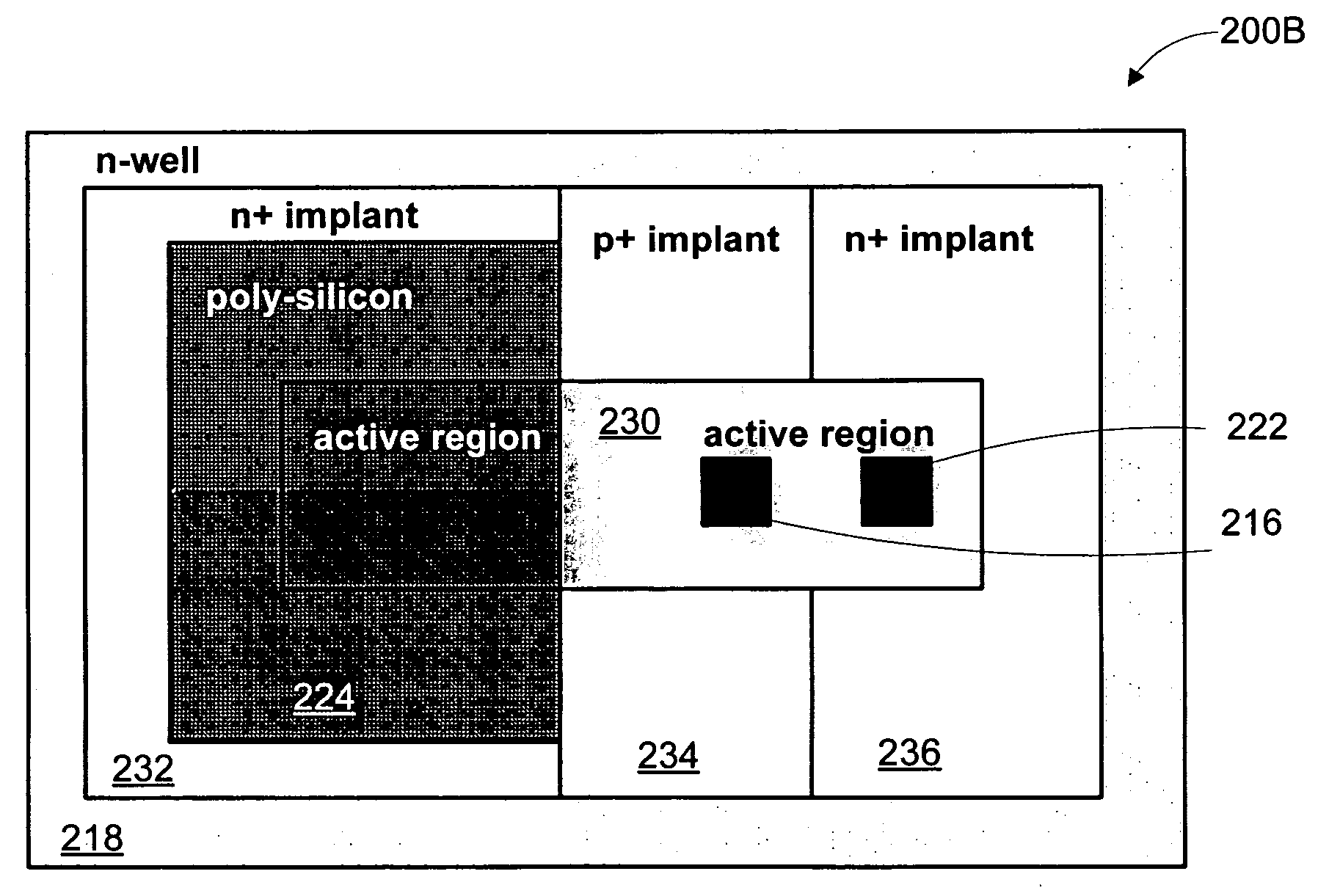
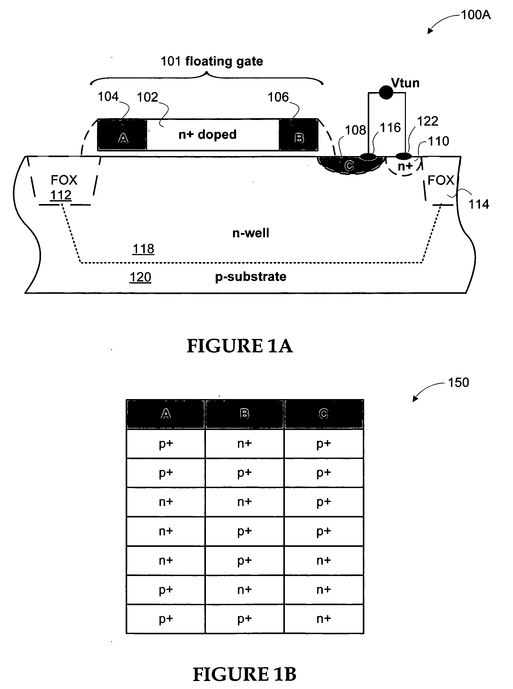
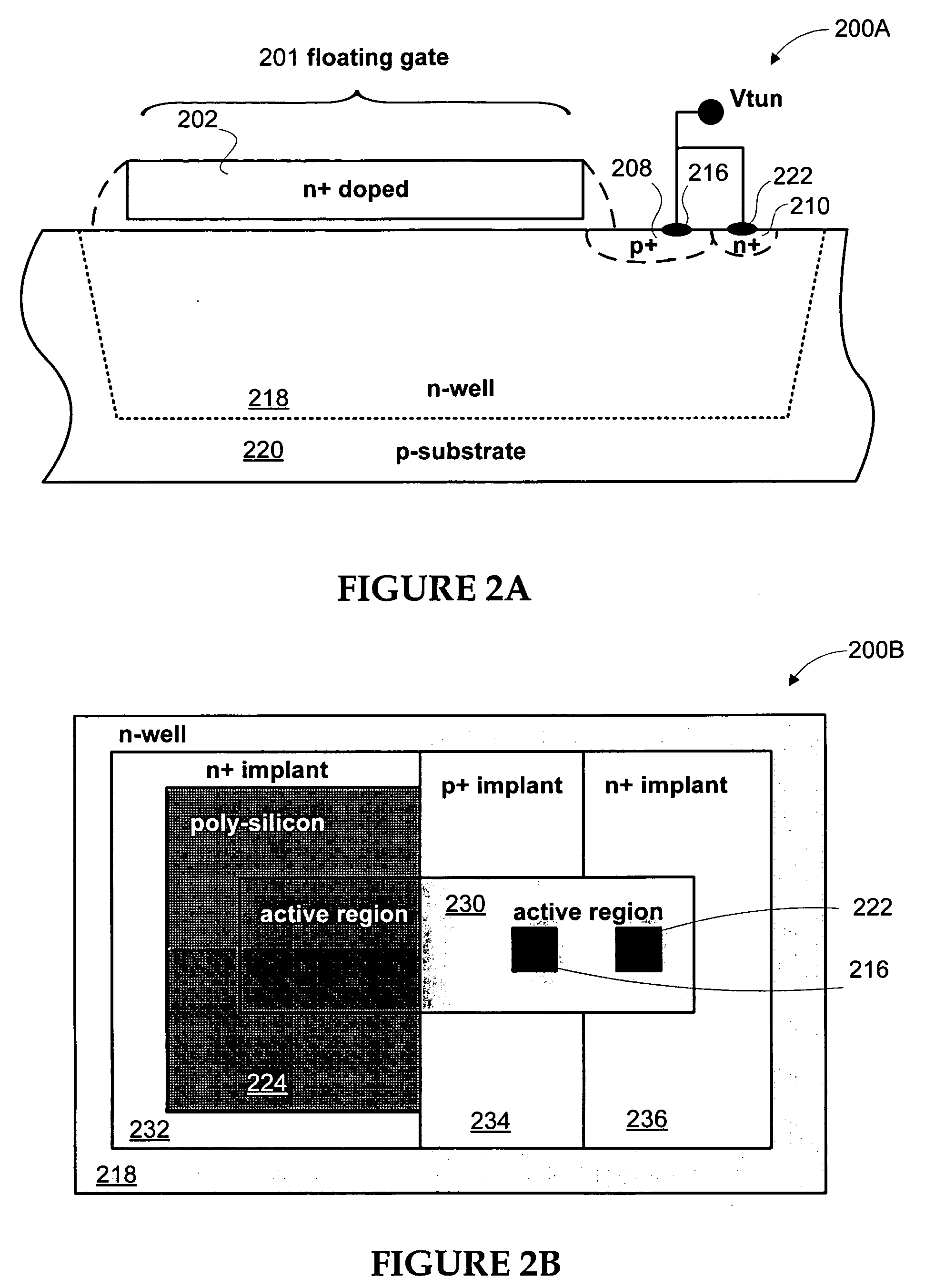
[0028] Various embodiments of the present invention will be described in detail with reference to the drawings, where like reference numerals represent like parts and assemblies throughout the several views. Reference to various embodiments does not limit the scope of the invention, which is limited only by the scope of the claims attached hereto. Additionally, any examples set forth in this specification are not intended to be limiting and merely set forth some of the many possible embodiments for the claimed invention.

[0029] Throughout the specification and claims, the following terms take at least the meanings explicitly associated herein, unless the context clearly dictates otherwise. The meanings identified below are not intended to limit the terms, but merely provide illustrative examples for the terms. The meaning of “a,”“an,” and “the” includes plural reference, the meaning of “in” includes “in” and “on.” The term “connected” means a direct electrical connection between the...


PUM


Abstract

Tunneling-enhanced, floating gate semiconductor devices and methods for forming such devices are described. In one embodiment, a p-n junction device is formed with a floating gate that is partially doped with n- and p-type impurities. Two regions on either side of an n+ doped region in the floating gate and a surface region on a substrate are implanted with the impurities based on a number of predetermined configurations. In another embodiment, a transistor type semiconductor device is configured with implanted impurities in two regions of its floating gate as well as two surface regions in its substrate. Enhanced tunneling junction enables use of lower tunneling voltages in applications such as programming NVM cells.

Description

RELATED APPLICATIONS [0001] This application claims the benefit of U.S. Provisional Application Ser. No. 60 / 667,188 filed on Mar. 30, 2005, which is hereby claimed under 35 U.S.C. § 119(e). The referenced Provisional Application and related U.S. Utility application Ser. No. 10 / 813,907 (IMPJ-0027A) filed on Mar. 30, 2004; Ser. No. 10 / 814,866 (IMPJ-0027B) filed on Mar. 30, 2004; Ser. No. 10 / 814,868 (IMPJ-0027C) filed on Mar. 30, 2004; and Ser. No. 11 / 095,938 (IMPJ-0083) filed on Mar. 30, 2005 are incorporated herein by reference. Furthermore, this application may be found to be related to U.S. Utility application Ser. No. 10 / 356,645 (IMPJ-0018) filed on Jan. 31, 2003.FIELD OF THE INVENTION [0002] The present invention relates to semiconductor devices, and more particularly, to devices and methods of forming such devices for providing tunneling-enhanced floating gate operations, to assist charge storing devices. BACKGROUND OF THE INVENTION [0003] Memory elements may be classified in tw...

Claims


Application Information

Patent Timeline
Patent Type & Authority Applications(United States)
IPC IPC(8): H01L29/788
CPCG11C16/0416G11C16/0441G11C16/045G11C2216/10H01L29/7883H01L27/11521H01L27/11558H01L29/42324H01L27/115H10B69/00H10B41/30H10B41/60
Inventor WANG, BINMA, YANJUN
Owner VIRAGE LOGIC
Why Eureka
Try Eureka