Electronic component mounting package and package assembled substrate

Inactive Publication Date: 2006-10-05
SANYO ELECTRIC CO LTD
View PDF4 Cites 33 Cited by
  • Summary
  • Abstract
  • Description
  • Claims
  • Application Information

AI Technical Summary

Benefits of technology

[0020] As described above, according to the electronic component mounting package and the package assembled substrate of the present invention, a flat surface can be obtained for a pair of external electr

Problems solved by technology

Therefore, there has been a problem of the package 83 shifting during a process for mounting the light emitting device on a mother board with solder reflo

Method used


Image

  • Electronic component mounting package and package assembled substrate
  • Electronic component mounting package and package assembled substrate
  • Electronic component mounting package and package assembled substrate

Examples


Example

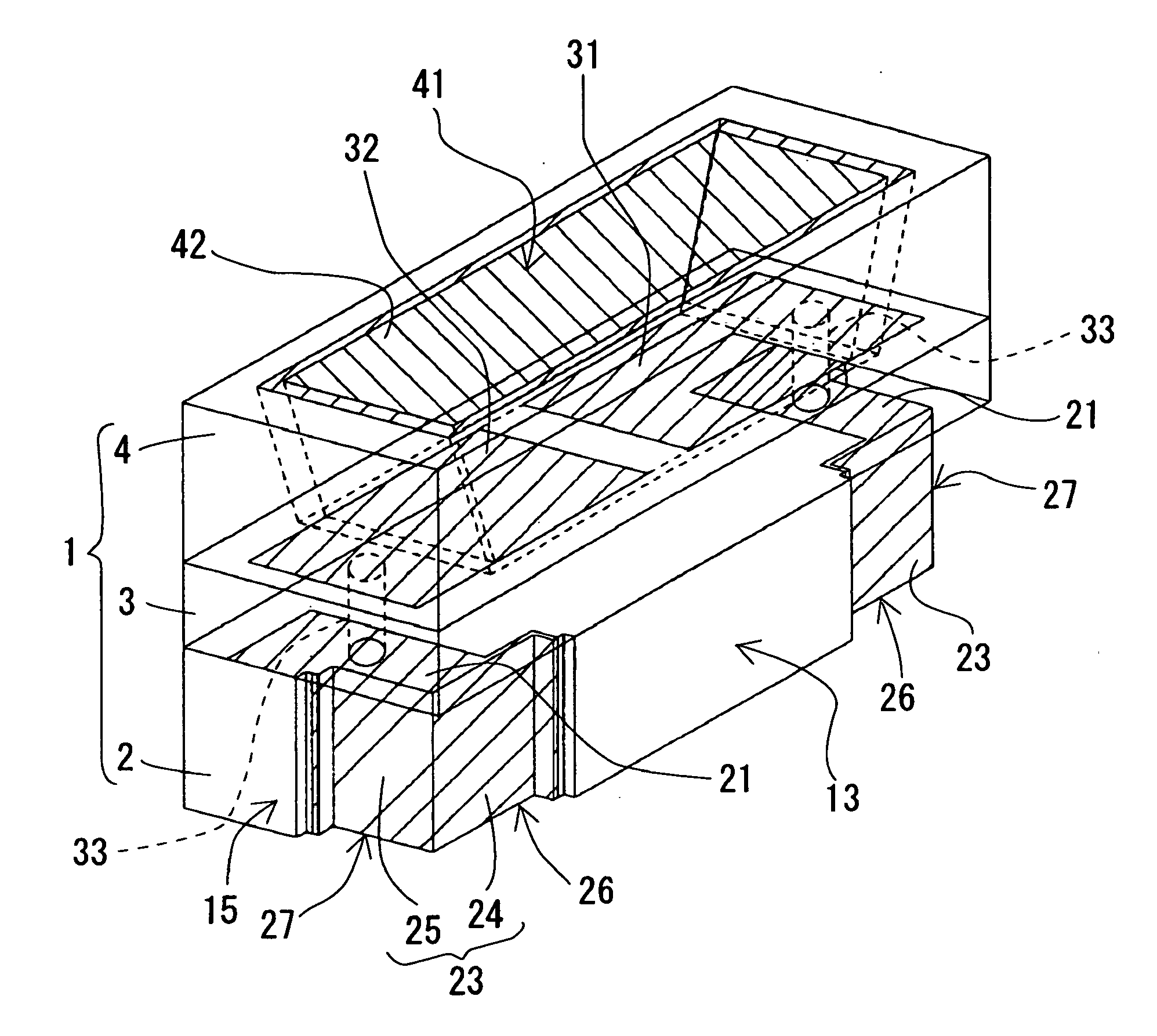
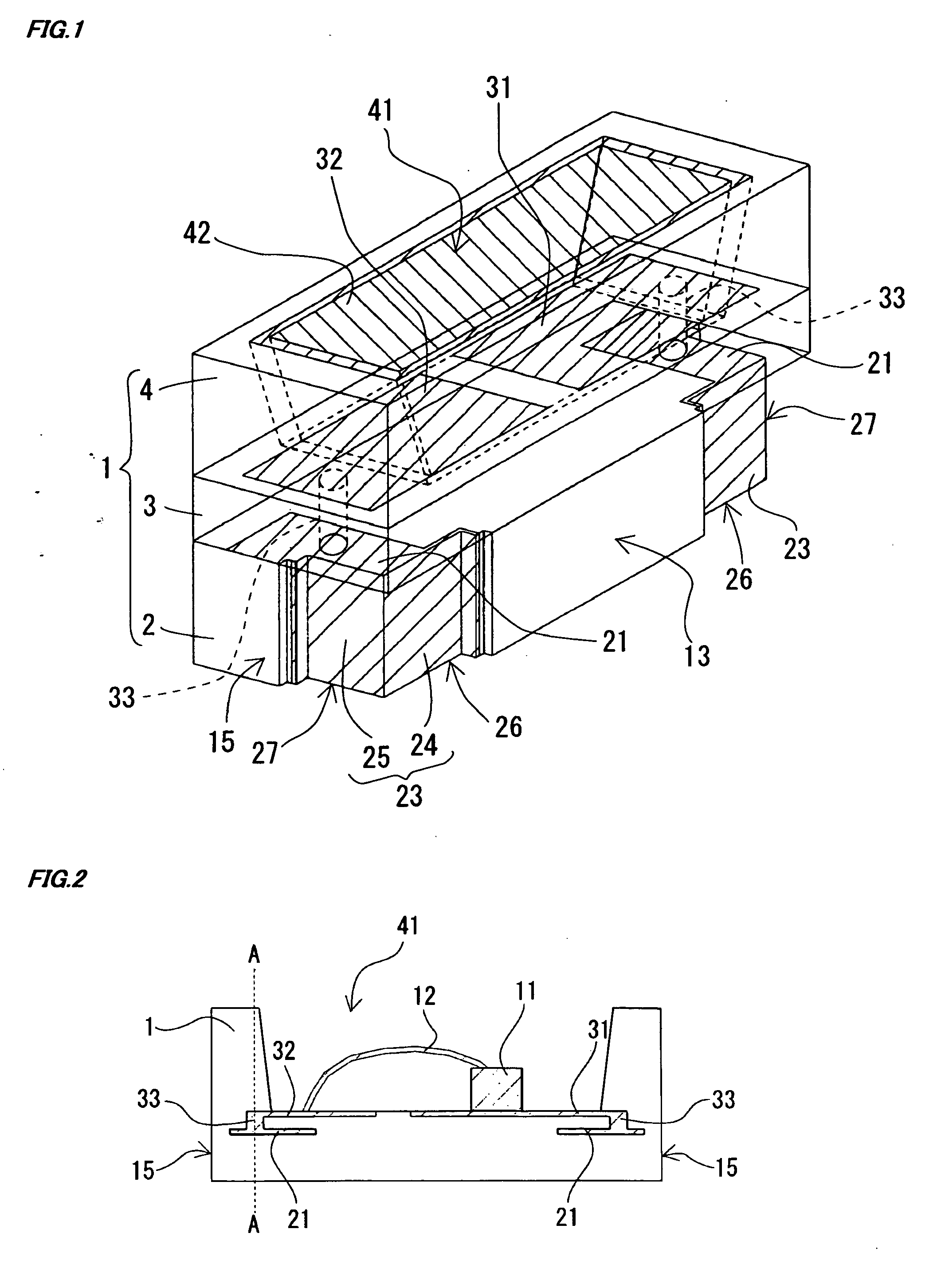
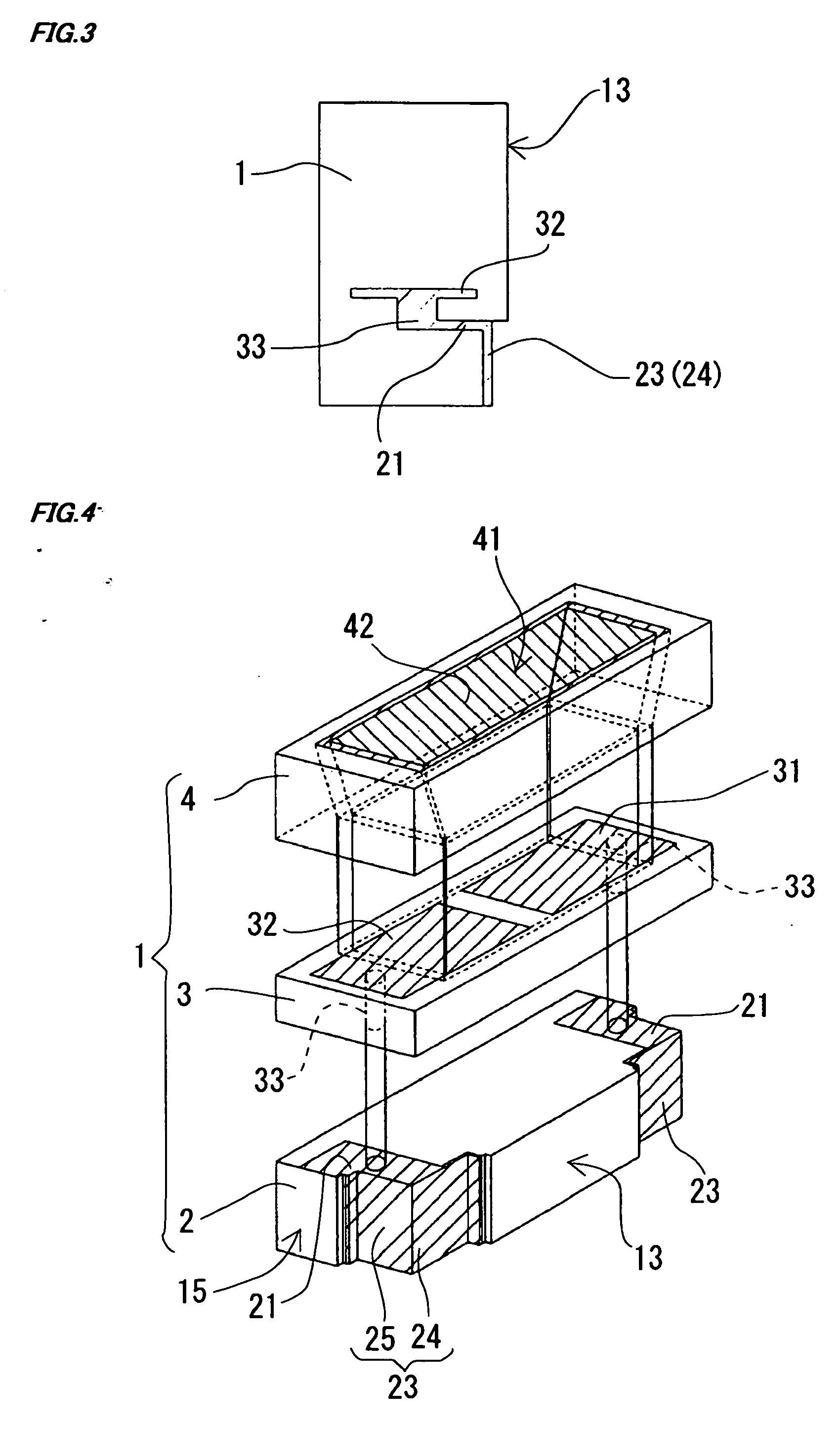
[0035] The present invention carried out in a light emitting device will be specifically described below with reference to the drawings. As shown in FIG. 2, the light emitting device of the present invention has a light emitting element 11, made of an LED, mounted on a surface of a package 1, and is placed, when mounted on a mother board 9 as shown in FIG. 11, such that the light emitting direction of the light emitting element 11 is parallel with a surface of the mother board 9.

[0036] As shown in FIG. 1 and FIG. 4, the package 1 is formed by laminating a first ceramic layer 2, a second ceramic layer 3 and a third ceramic layer 4, and has a mount surface 13 to be a joint surface when mounted on the mother board 9, defined on a side surface parallel with the laminating direction. In a mounted state, a pair of side surfaces 15, 15 provided at both sides of the mount surface 13 will be perpendicular to the surface of the mother board 9.

[0037] The third ceramic layer 4 has a cavity 41...


PUM


Abstract

A package of the present invention has a laminate structure formed by laminating a plurality of ceramic layers, and has a mount surface to be a joint surface when mounted on a mother board, defined parallel with the laminating direction. A first ceramic layer has a recess with an L-shaped cross section across the mount surface and a side surface, defined at each end thereof in a direction perpendicular to the laminating direction, and an external electrode formed on each recess, the external electrode having a surface thereof exposed to the mount surface.

Description

[0001] The priority application Number 2005-075145 upon which this patent application is based is hereby incorporated by reference. BACKGROUND OF THE INVENTION [0002] 1. Field of the Invention [0003] The present invention relates to an electronic component mounting package having a laminate structure of a plurality of ceramic layers, and to a package assembled substrate, which is an intermediate product thereof. [0004] 2. Description of Related Art [0005] A light emitting device as shown in FIG. 12 has been conventionally known in which a light emitting element 11 such as an LED is mounted in a package 8 formed by laminating a plurality of ceramic layers (JP 2002-232017, A). The package 8 is provided with a cavity 81 for housing the light emitting element 11. A first land layer 8a and a second land layer 8b are formed with a conductive material such as silver on the bottom surface of the cavity 81. A power supply terminal (not shown) provided on the top surface of the light emitting...

Claims


Application Information

Patent Timeline
IPC IPC(8): H01L23/02
CPCH01L33/486H01L33/62H01L2224/48091H01L2924/12041H01L2224/48227H01L2924/00014
Inventor HONGO, MASANORIFUKUYAMA, MASAMI
Owner SANYO ELECTRIC CO LTD
Why Eureka
Try Eureka