
Program-verify method of non-volatile memory device

a non-volatile memory and verification method technology, applied in static storage, digital storage, instruments, etc., can solve the problems of degrading the read margin and adversely affecting the in-cycling and retention characteristics of the margin, and achieve the effect of reducing the threshold voltage distribution

Active Publication Date: 2006-10-12
SK HYNIX INC
View PDF9 Cites 41 Cited by
  • Summary
  • Abstract
  • Description
  • Claims
  • Application Information

AI Technical Summary

Benefits of technology

[0008] The present invention relates to a method of programming non-volatile memory device. An embodiment of the present invention is directed to reduce the threshold voltage distribution among the program cells by applying different progra

Problems solved by technology

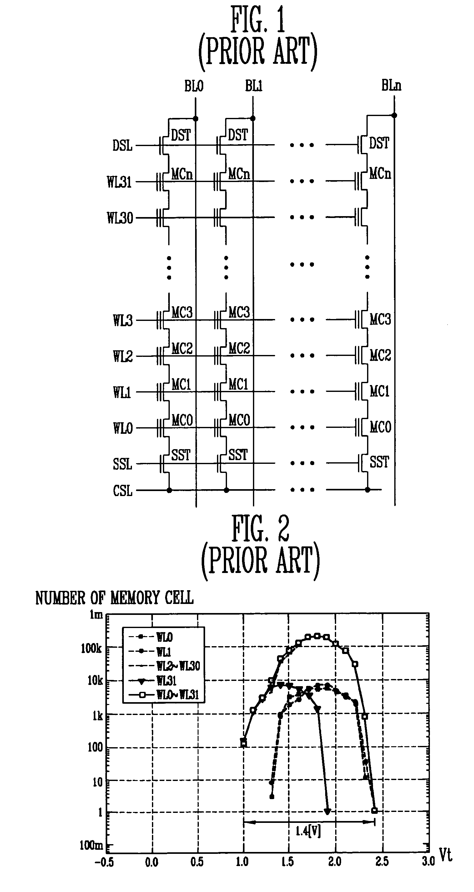
This increased threshold voltage differences among memory cells may degrade a read margin in single level cells or multi-level cells and may also have an adverse effect on margin in-cycling and retention characteristics.

Method used


Image

  • Program-verify method of non-volatile memory device
  • Program-verify method of non-volatile memory device
  • Program-verify method of non-volatile memory device

Examples


Embodiment Construction

[0017] In the following detailed description, only certain exemplary embodiments of the present invention have been shown and described for illustrative purposes. As those skilled in the art will realize, the described embodiments may be modified in various different ways without departing from the spirit or scope of the present invention. Accordingly, the drawings and description are to be regarded as illustrative in nature and not restrictive. Like reference numerals designate like elements.

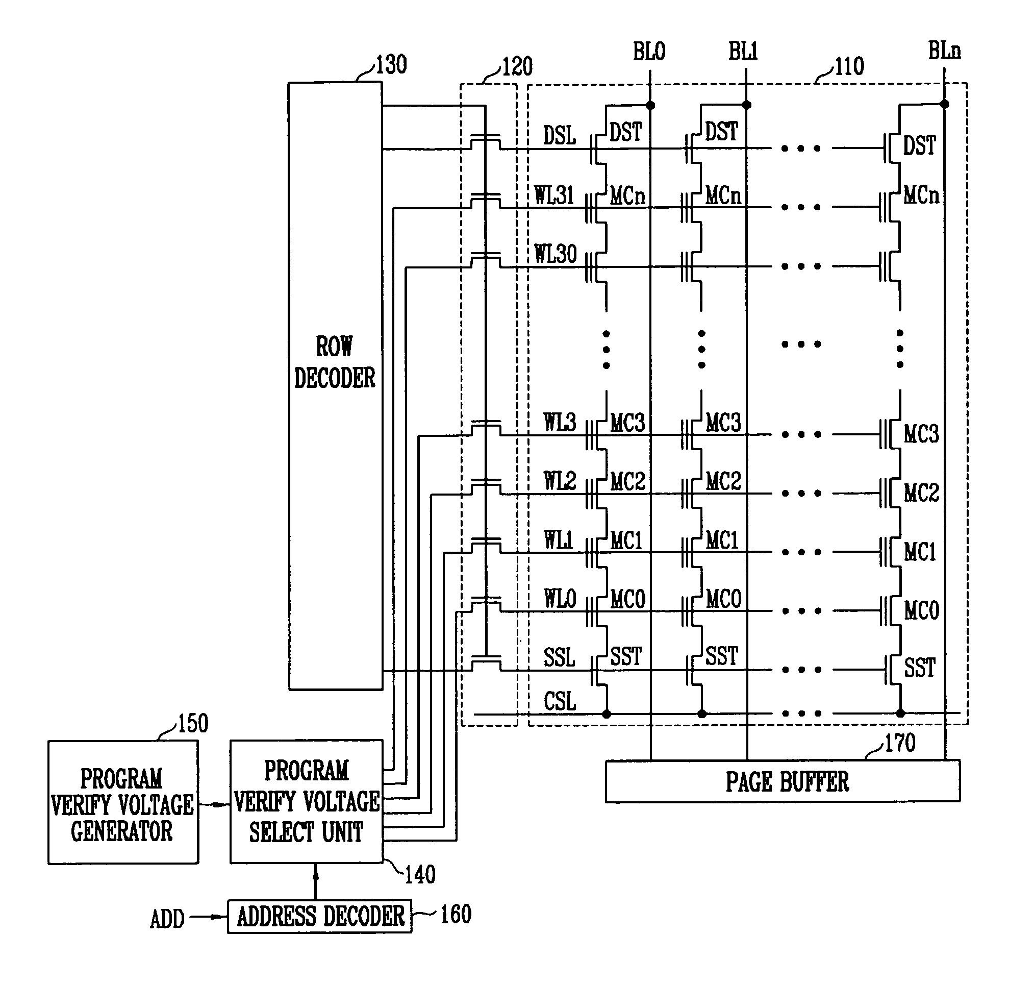
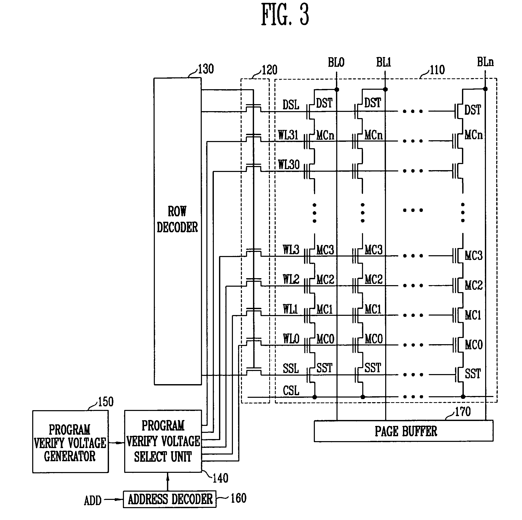
[0018]FIG. 3 is a block diagram showing a NAND flash memory device in which the threshold voltage distribution of memory cells can be narrowed according to one embodiment of the present invention.

[0019] Referring to FIG. 3, the NAND flash memory device includes a memory cell block 110, a word line switching unit 120, a row decoder 130, a program-verify voltage select unit 140, a program-verify voltage generator 150, an address decoder 160 and a page buffer 170.

[0020] Referring to FIG. 3, the...


PUM


Abstract

A method for programming a non-volatile memory device includes applying a first program-verify voltage to a first word line to determine whether or not memory cells associated with the first word line have been programmed successfully. A second program-verify voltage is applied to a second word line to determine whether or not memory cells associated with the second word line have been programmed successfully. The second program-verify voltage is different from the first program-verify voltage. The first and second word lines are associated with the same word line switching unit.

Description

BACKGROUND [0001] The present invention relates to a method of programming a non-volatile memory device. More particularly, the present invention relates to a program-verify method. [0002] In general, there is an increasing demand for non-volatile memory devices which can be electrically programmed and erased and do not need the refresh function of rewriting data at regular intervals. The term “program” refers to the operation of writing data into the memory cells. [0003] To increase the level of integration of memory devices, a NAND flash memory device in which a plurality of memory cells are connected in series (i.e., a structure in which neighboring cells share the drain or source) to form one string has been developed. The NAND flash memory device is a memory that sequentially reads information unlike the NOR flash memory device. [0004] The distribution of threshold voltages (Vt) for cells being programmed (or program cells) in conventional NAND flash memory device at least part...

Claims


Application Information

Patent Timeline
IPC IPC(8): G11C11/34
CPCG11C16/3454G11C16/0483G11C16/34
Inventor LEE, MIN KYU
Owner SK HYNIX INC
Learn More