Method for forming anti-stiction bumps on a micro-electro mechanical structure

a micro-electro mechanical structure and anti-stiction technology, applied in the direction of microstructural technology, microstructure devices, electric devices, etc., can solve the problems of in-use stiction, less capable and versatile processes, and more difficult problems to address

Active Publication Date: 2006-10-19
DELPHI TECH IP LTD
View PDF1 Cites 12 Cited by
  • Summary
  • Abstract
  • Description
  • Claims
  • Application Information

AI Technical Summary

Problems solved by technology

A more difficult problem to address is in-use stiction, which occurs during operation when components of the microstructure come into contact, intentionally or accidentally.
However, these processes are generally less capable and versatile than surface micromachining, in terms of device function.
However, even bulk micromachined MEM devices may still experience in-use stiction.
However, the use of siloxan SAMs is difficult to implement because of the chemistry and, as such, its poor reproducibility limits its practical usage.
In addition, many organic layers have a limited lifetime or decrease the allowable operating temperature of the device.
However, this technique cannot be utilized for silicon-on-insulator (SOI) wafer based MEM devices, as the sacrificial layer is part of the SOI wafer.

Method used


Image

  • Method for forming anti-stiction bumps on a micro-electro mechanical structure
  • Method for forming anti-stiction bumps on a micro-electro mechanical structure
  • Method for forming anti-stiction bumps on a micro-electro mechanical structure

Examples


Embodiment Construction

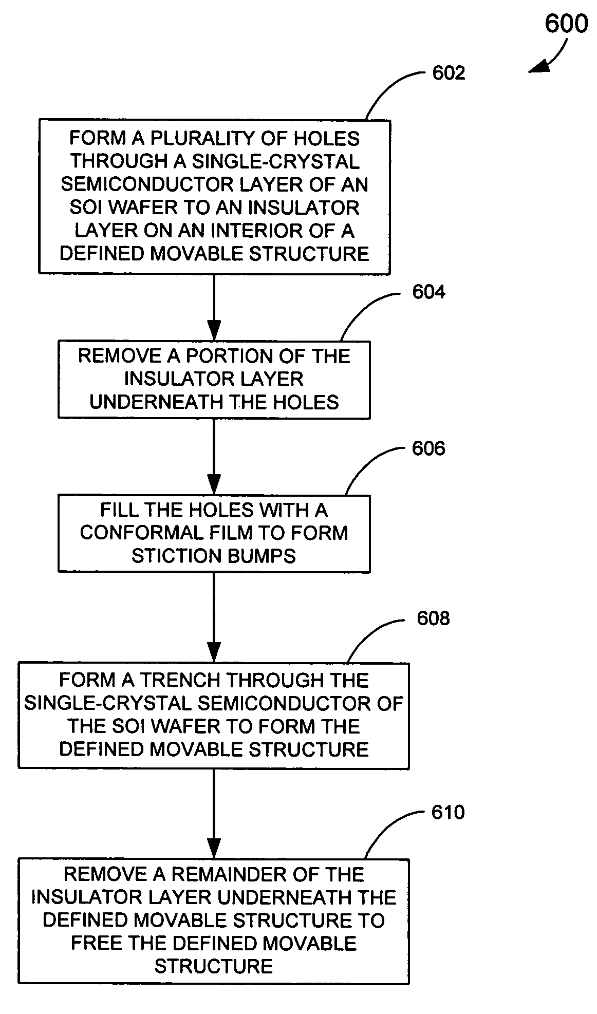
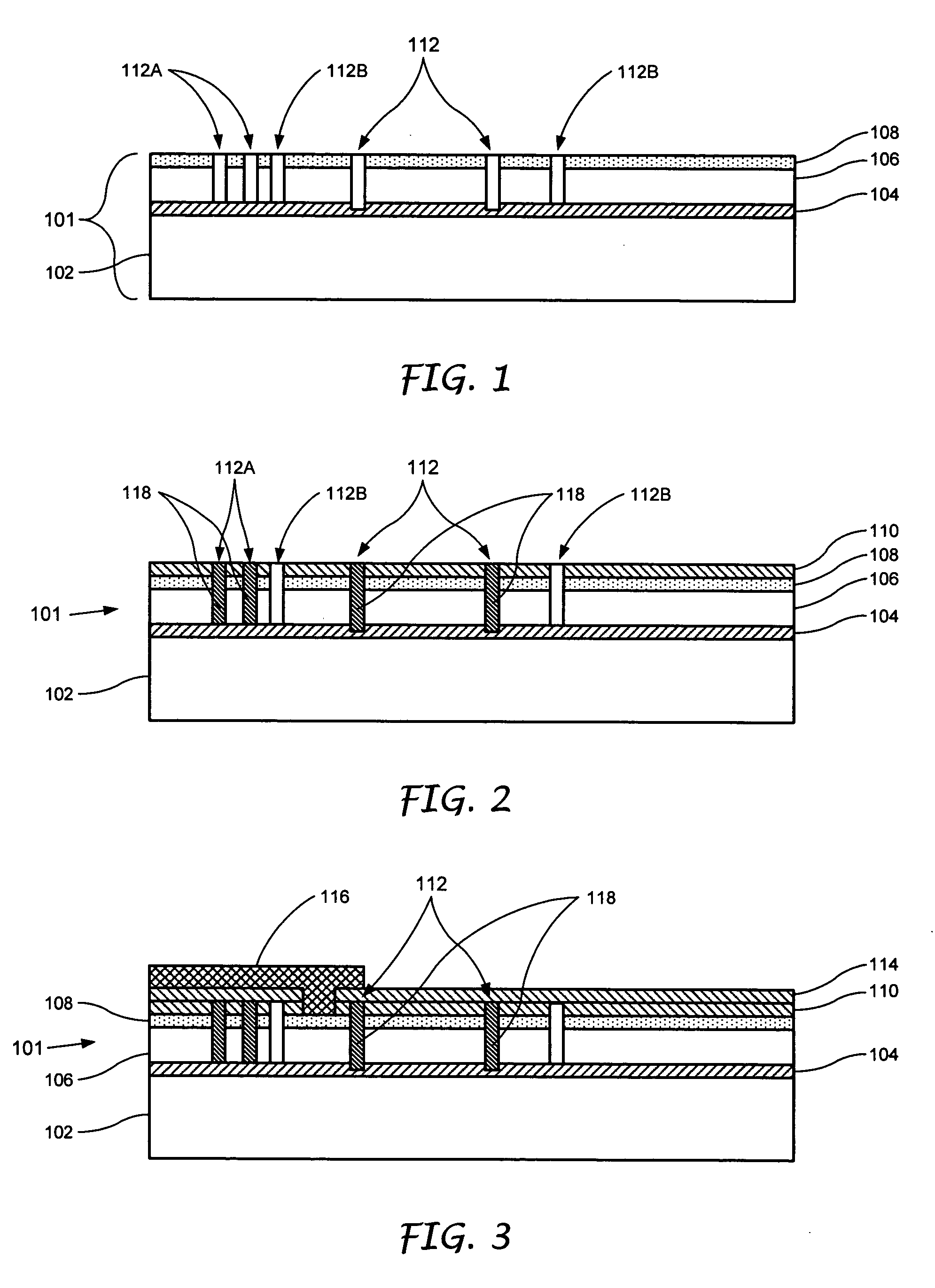
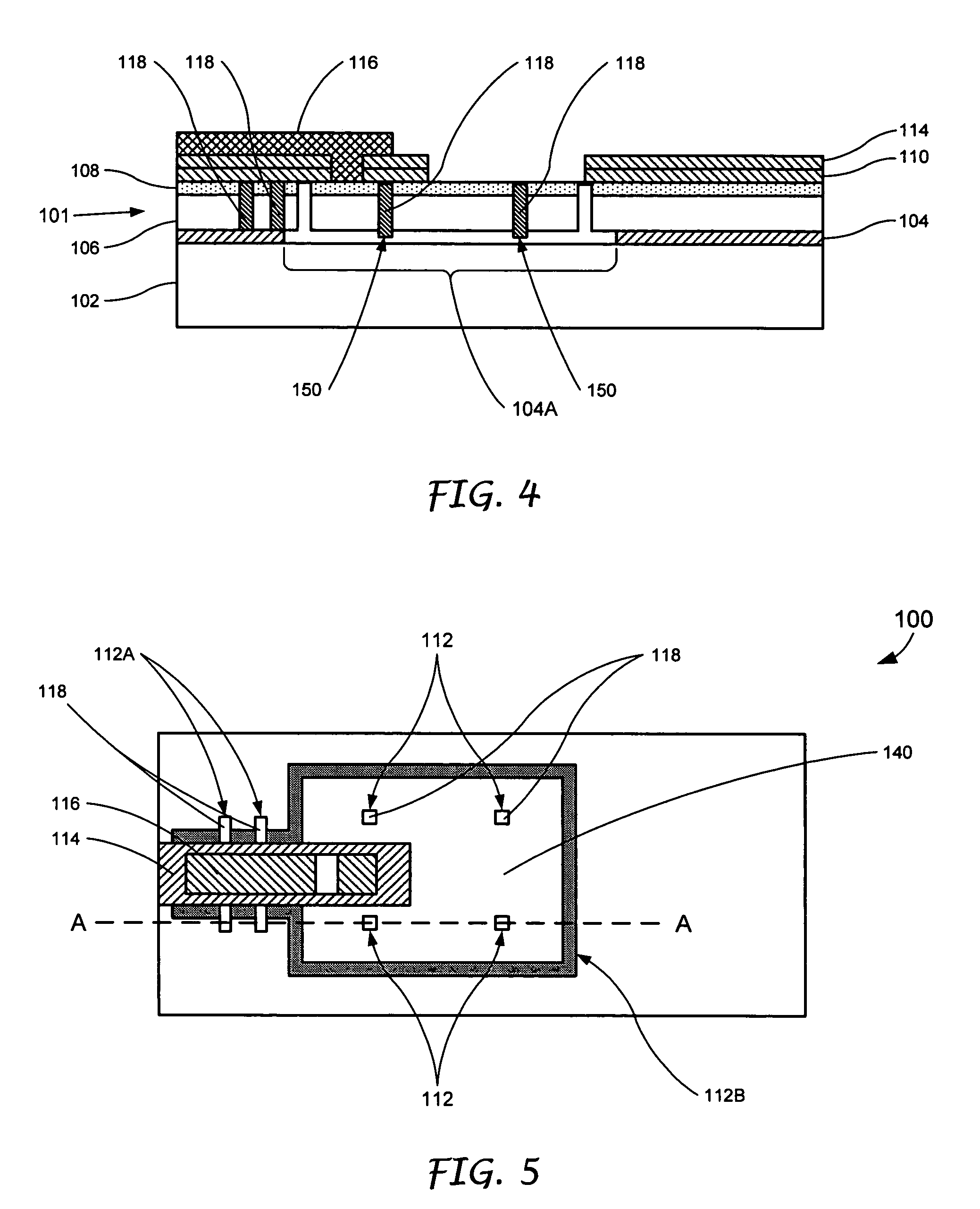
[0014] According to one embodiment of the present invention, a micro-electro mechanical (MEM) device is fabricated from a silicon-on-insulator (SOI) wafer, which includes a support substrate, e.g., a single-crystal silicon substrate, bonded to a single-crystal semiconductor layer via an insulator layer, e.g., an oxide layer. One or more trenches (holes) are etched, e.g., with a deep reactive ion etch (DRIE), through a defined movable structure of the MEM device until the holes reach the oxide interface of the SOI wafer. A dry or wet oxide etch is then performed to partially remove the oxide underneath the holes. Next, a conformal film, such as a polysilicon, is used to fill the holes, including the region at the bottom of the holes, where the oxide was removed. A remainder of the oxide layer, underneath the defined movable structure, is removed during an undercut step to free the movable structure. As such, the conformal film, which extends below a lower surface of the movable struc...


PUM


Abstract

A technique for forming anti-stiction bumps on a bottom surface of a micro-electro mechanical (MEM) structure includes a number of process steps. The MEM structure is fabricated from an assembly that includes a support substrate bonded to a single-crystal semiconductor layer, via an insulator layer. A plurality of holes are formed through the single-crystal semiconductor layer to the insulator layer on an interior portion of a defined movable structure. A portion of the insulator layer underneath the holes is removed. The holes are then filled with a conformal film that extends below a lower surface of the defined movable structure to provide a plurality of anti-stiction bumps. A trench is then formed through the single-crystal semiconductor layer to the insulator layer to form the defined movable structure. Finally, a remainder of the insulator layer underneath the defined movable structure is removed to free the defined movable structure.

Description

TECHNICAL FIELD [0001] The present invention is generally directed to a method for forming anti-stiction bumps and, more specifically, to a method for forming anti-stiction bumps on a bottom surface of a micro-electro mechanical structure. BACKGROUND OF THE INVENTION [0002] Microstructure stiction frequently occurs in micro-electro mechanical (MEM) devices due to wet chemical processing of the microstructure. Typically, stiction occurs when surface adhesion forces are higher than the mechanical restoring force of the microstructure. For example, stiction may occur after wet etching of an underlying sacrificial layer, when a liquid meniscus formed on hydrophilic surfaces of the microstructure pull the microstructure toward an associated substrate. Usually, such stiction problems may be alleviated by a dry hydrofluoric (HF) etching or supercritical carbon dioxide (CO2) drying. [0003] A more difficult problem to address is in-use stiction, which occurs during operation when components ...

Claims


Application Information

Patent Timeline
Patent Type & Authority Applications(United States)
IPC IPC(8): H01L21/00
CPCB81B3/001
Inventor CHILCOTT, DAN W.
Owner DELPHI TECH IP LTD
Why Eureka
Try Eureka