Pixel defect correction device

a defect correction and defect technology, applied in the field of pixel defect correction devices, can solve the problems of noise, inconsistent sensitivities of respective pixels, and charge then leakage into adjacent pixels, and achieve the effect of improving the accuracy of correction of defective pixels

Inactive Publication Date: 2006-10-26
MONUMENT PEAK VENTURES LLC
View PDF20 Cites 47 Cited by
  • Summary
  • Abstract
  • Description
  • Claims
  • Application Information

AI Technical Summary

Benefits of technology

[0019] According to the present invention, a correction method is modified so as to use different pixels in corre...

Problems solved by technology

The charge then leaks into the adjacent pixels, becoming noise.
With such noise, or electric charge invading into pixels having B or G small filters, the sensitivities of the respective pixels become inconsistent, even when an image of a uniformly colored object having no pattern is captured.
Defective pixels of an image capturing element, such as a CCD, may inconsistently increase or decrease due to, for example, increased temperature, long time exposure, and so forth.
However, use of the pixels adjacent to the focused pixel cannot guarantee accurate detection and correction due to the influence of line crawl.
When the difference between the estimated and actual pixel values of the pixel Gorg is...

Method used


Image

  • Pixel defect correction device
  • Pixel defect correction device
  • Pixel defect correction device

Examples


Embodiment Construction

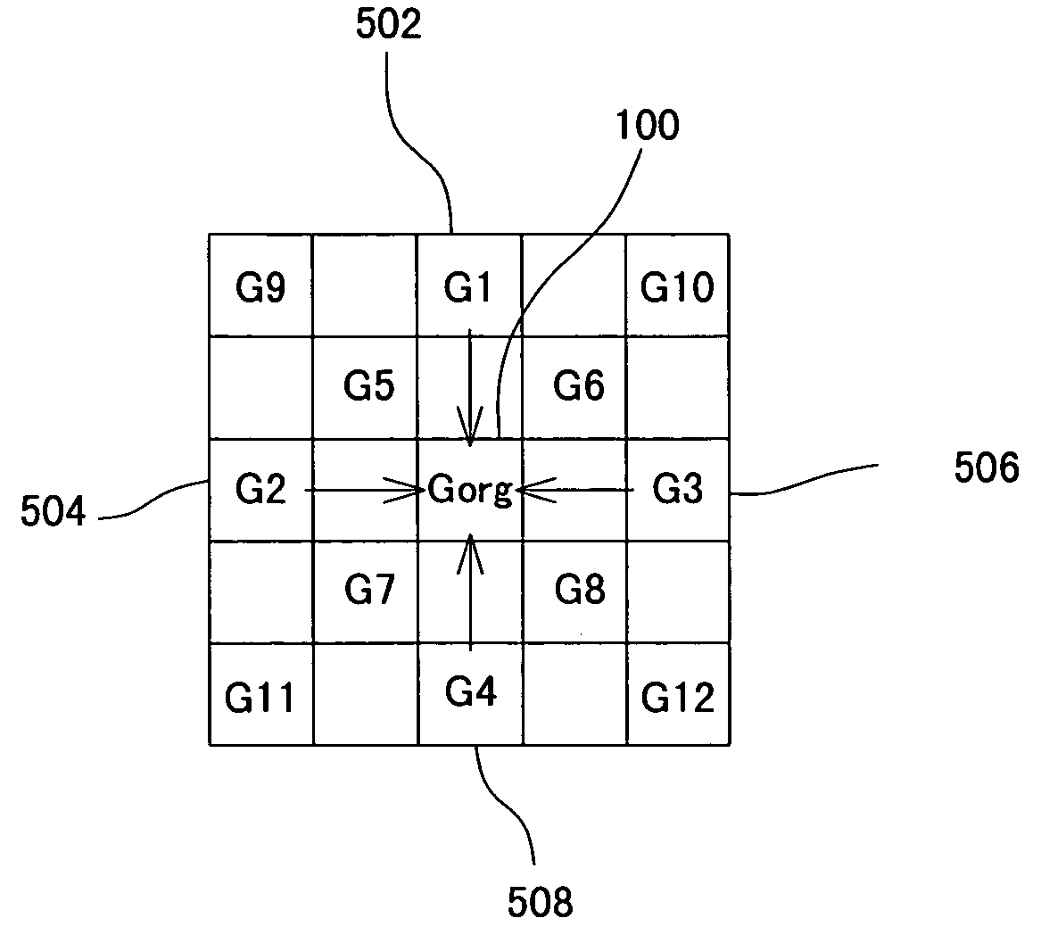
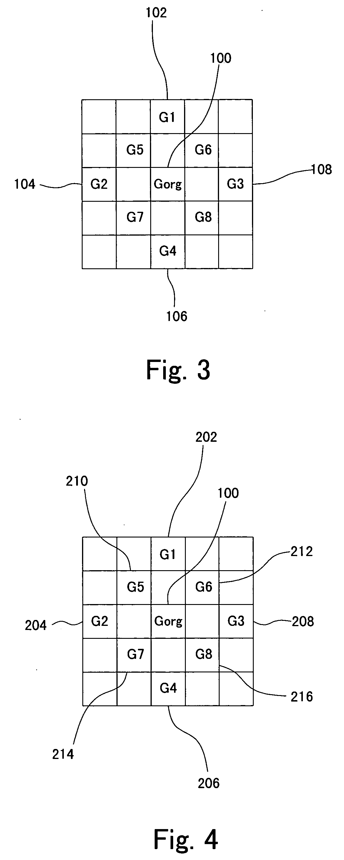
[0035] In the following, a preferred embodiment of the present invention will be described while referring to a Bayer array as an example, based on the accompanied drawings.

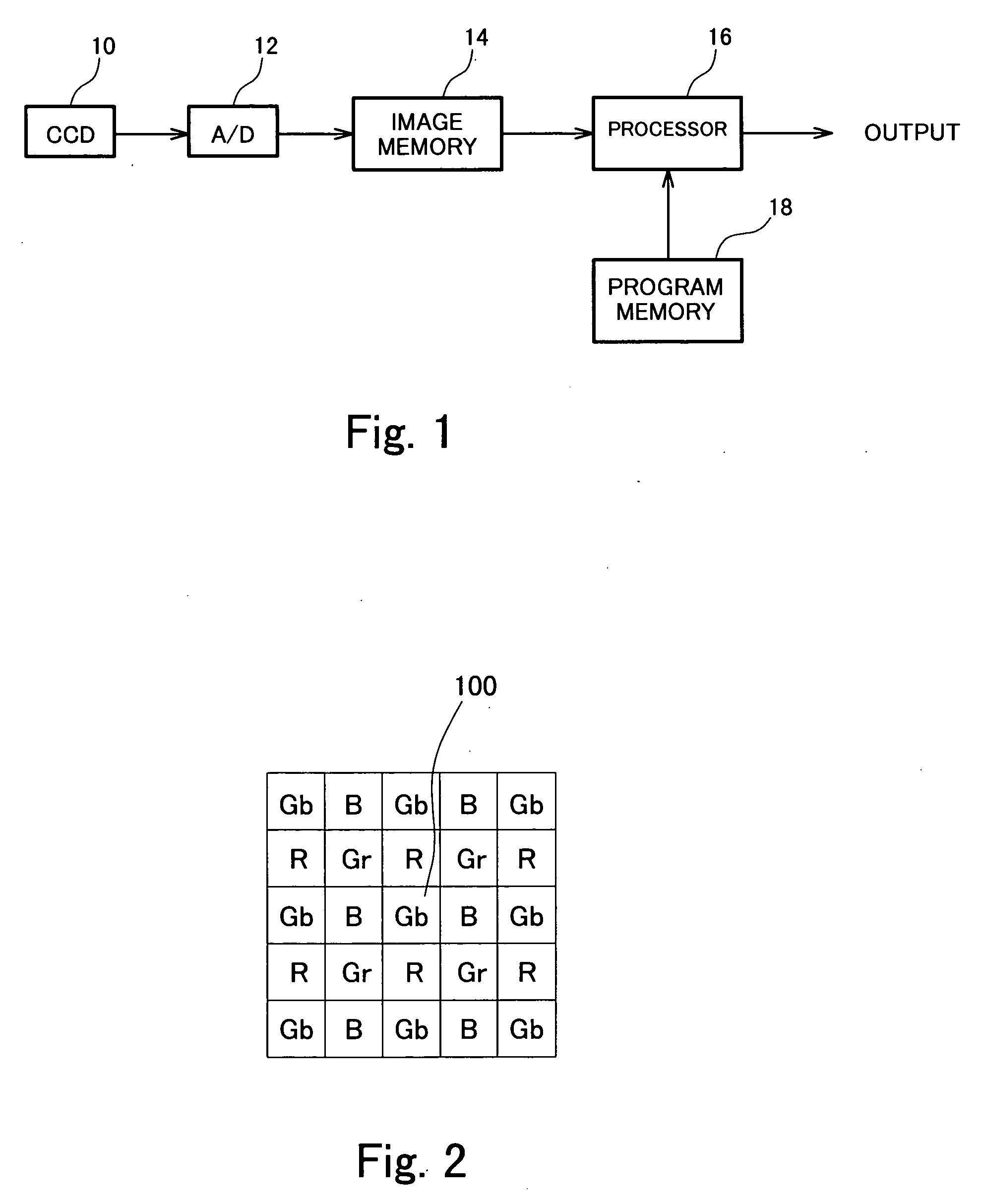
[0036]FIG. 1 is a structural block diagram for a digital camera according to the embodiment. In the drawing, components including an optical system including a lens, a shutter, and so forth; a display device; and various switches are omitted for clarity, as such components are well known.

[0037] A CCD 10 has a color filter in a Bayer array, and photoelectrically converts the image of an object before outputting a pixel signal for an R pixel, a G pixel, and a B pixel. An A / D 12, having received an analogue pixel signal from the CCD 10, converts the signal into a digital signal which it then outputs as a pixel value to a subsequent image memory 14. The image memory 14 sequentially stores the respective pixel values. A processor 16 sequentially reads out the pixel values from the image memory 14 and carries out def...


PUM


Abstract

To enhance accuracy in correction of a defective pixel. An image of an object is captured using a digital camera, and stored in an image memory 14. A processor 16 detects a defect, using pixels located in the vertical and horizontal directions relative to, in lines of the same color as, and separated by one line from, the focused line. With any defect found, the presence or absence of line crawl is next determined. When it is determined that line crawl is present, the presence or absence of a diagonal edge is then determined. Subsequently, the surrounding pixels used to correct a defective pixel are selected in consideration of whether or not line crawl or a diagonal edge are present.

Description

FIELD OF THE INVENTION [0001] The present invention relates to a device for correcting a defect which is present in a group of pixels supplied with image data obtained using an image capturing device such as a CCD. BACKGROUND OF THE INVENTION [0002] Conventional techniques for detecting a defective pixel in a two dimensional image capturing element such as a CCD, and correcting the defective pixel by utilizing the pixels around that pixel, are known. [0003] Japanese Patent Laid-open Publication No. Hei 9-238355 discloses a technique for removing line crawl by outputting a Gb in a Bayer array after being multiplied by a line crawl correction, and outputting Gr intact. [0004]“Line crawl” is a phenomena which may occur under the following conditions. That is, when a color filter comprising R, G, B small color filters in a Bayer array is provided on a light receiving filter, a long wavelength light which has passed through an R small color filter reaches a deeper site under the light re...

Claims


Application Information

Patent Timeline
IPC IPC(8): H04N5/217H04N5/335H04N5/367H04N5/372H04N9/07
CPCH04N5/367H04N25/68
Inventor SATO, HIDEHIKOYOSHIKAWA, SUMITO
Owner MONUMENT PEAK VENTURES LLC
Why Eureka
Try Eureka