Terminal pad structures and methods of fabricating same

a technology of terminal pads and structures, applied in the direction of electrical equipment, semiconductor devices, semiconductor/solid-state device details, etc., can solve the problems of increasing fabrication process costs, complex structures of conventional terminal pads, and affecting the fabrication process

Active Publication Date: 2006-11-09
GLOBALFOUNDRIES US INC
View PDF6 Cites 39 Cited by
  • Summary
  • Abstract
  • Description
  • Claims
  • Application Information

AI Technical Summary

Problems solved by technology

Conventional terminal pads are complex structures because of the structural strength and contamination seal the terminal pad must provide.
For integrated circuit chips for low cost or commodity products and such as used in wireless technology, conventional terminal pad structures and fabrication processes add significant costs to the fabrication process.

Method used


Image

  • Terminal pad structures and methods of fabricating same
  • Terminal pad structures and methods of fabricating same
  • Terminal pad structures and methods of fabricating same

Examples


Embodiment Construction

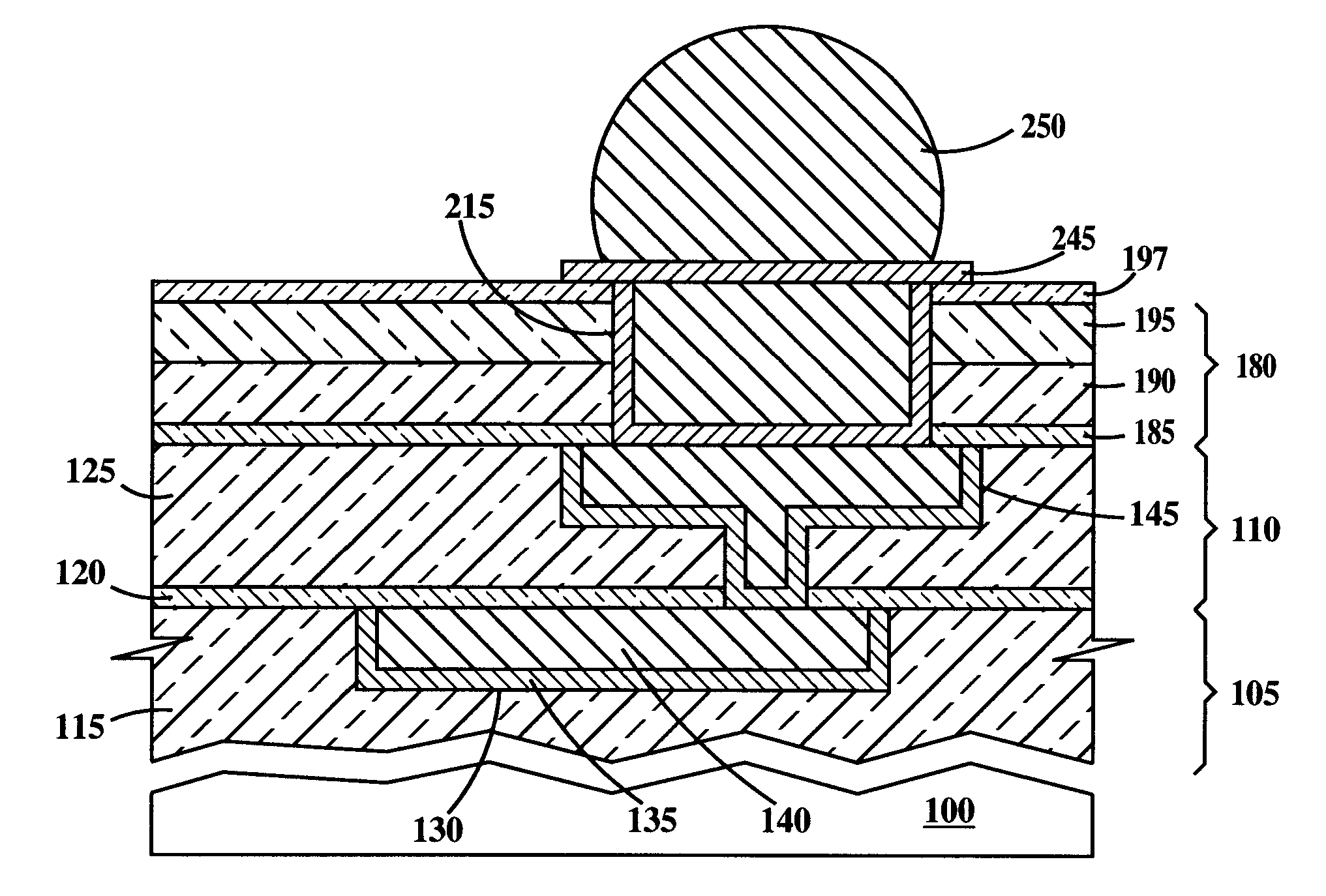
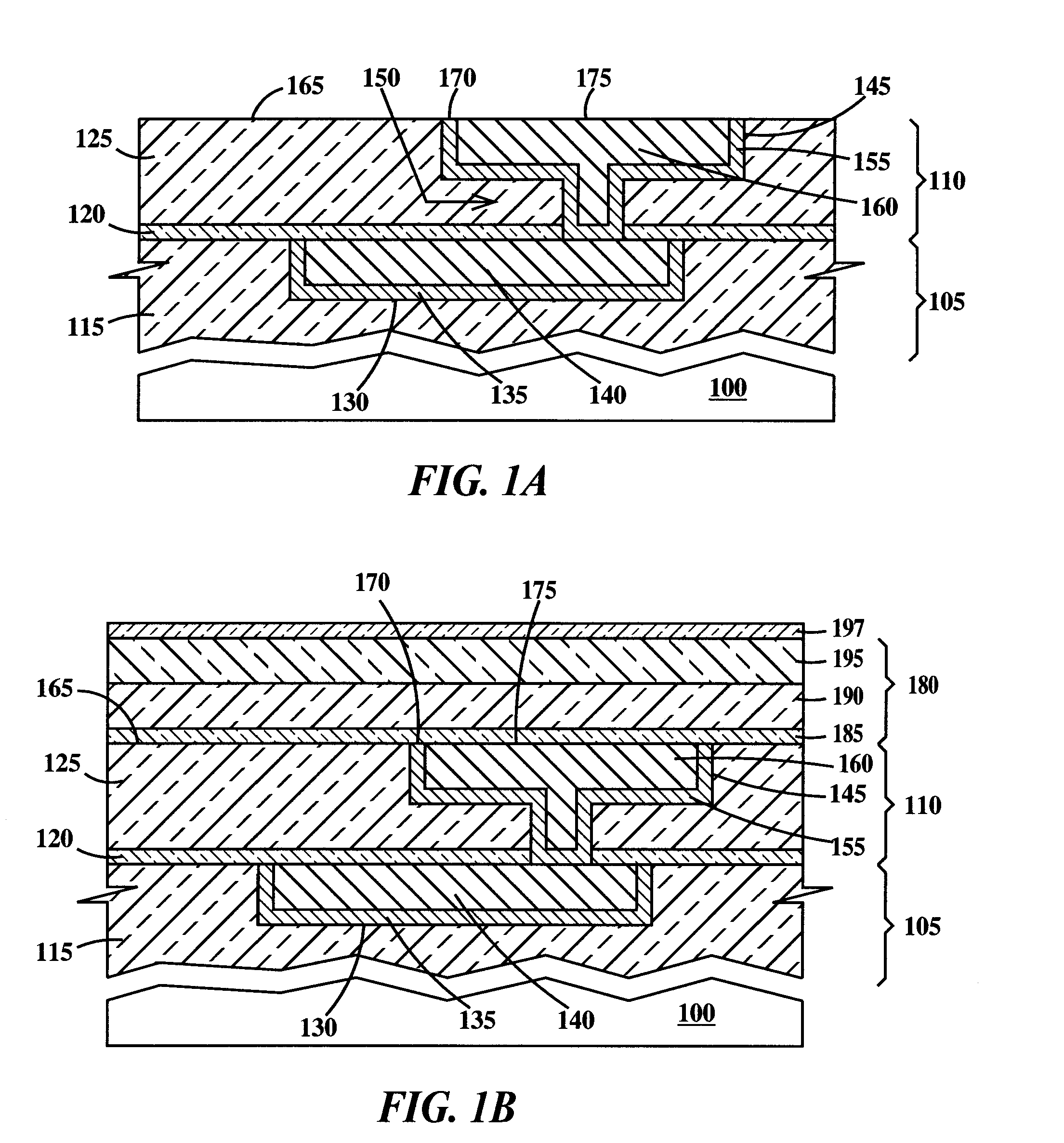
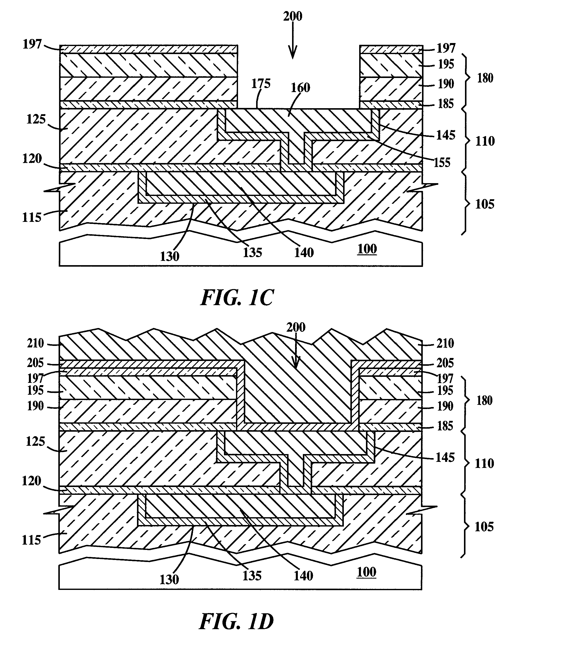
[0012]FIGS. 1A through 1F are cross-sectional views illustrating fabrication of a terminal pad structure according to a first embodiment of the present invention. FIG. 1A illustrates an exemplary integrated circuit chip prior to formation of a terminal pad according to the first embodiment of the present invention. In FIG. 1A formed on a substrate 100, are wiring levels 105 and 110. Wiring level 105 includes a dielectric layer 115. Wiring level 110 includes a dielectric layer 120 and a dielectric layer 125. Formed in dielectric layer 105 is a damascene wire 130 comprising an electrically conductive liner 135 and an electrically conductive core conductor 140. Formed in interlevel dielectric layer 110 is a damascene wire 145 and integral via 150 comprising an electrically conductive liner 155 and an electrically conductive core conductor 160. Top surface 165 of dielectric layer 125, top surface 170 of conductive liner 155 and top surface 175 of core conductor 160 are substantially cop...


PUM

PropertyMeasurementUnit
relative permittivityaaaaaaaaaa

Abstract

Terminal pads and methods of fabricating terminal pads. The methods including forming a conductive diffusion barrier under a conductive pad in or overlapped by a passivation layer comprised of multiple dielectric layers including diffusion barrier layers. The methods including forming the terminal pads subtractively or by a damascene process.

Description

FIELD OF THE INVENTION [0001] The present invention relates to the field of integrated circuits; more specifically, it relates to terminal pads for an integrated circuit and methods for fabricating the terminal pads. BACKGROUND OF THE INVENTION [0002] Integrated circuits include devices such as metal-oxide-silicon field effect transistors (MOSFETs) formed in a semiconductor substrate, interconnected into circuits by wires in interconnect layers formed on top of the substrate. At the highest or uppermost level of an integrated circuit chips, these wires must be connected to terminal pads which allow wirebond or solder bump connections to a next level of packaging, such as to a module or circuit board. Conventional terminal pads are complex structures because of the structural strength and contamination seal the terminal pad must provide. For integrated circuit chips for low cost or commodity products and such as used in wireless technology, conventional terminal pad structures and fa...

Claims


Application Information

Patent Timeline
Patent Type & Authority Applications(United States)
IPC IPC(8): B32B7/12
CPCH01L24/11H01L2224/05006H01L2924/0002H01L2224/0401H01L2224/05554H01L2224/02166H01L2924/00014H01L2924/0001H01L2224/45124H01L2224/13111H01L2224/131H01L2224/05007H01L2224/13022H01L2224/05022H01L2224/05568H01L2224/05572H01L2224/13007H01L2224/13099H01L2224/16H01L2924/01013H01L2924/01015H01L2924/01022H01L2924/01027H01L2924/01029H01L2924/01073H01L2924/01074H01L2924/01079H01L2924/01082H01L2924/04941H01L2924/04953H01L2924/13091H01L2924/14H01L2924/01019H01L2924/01024H01L2924/014H01L23/3192H01L24/03H01L24/05H01L24/13H01L2924/00H01L2224/48H01L2224/05552H01L2224/13023
Inventor COOLBAUGH, DOUGLAS D.EDELSTEIN, DANIEL C.ESHUN, EBENEZER E.HE, ZHONG-XIANGRASSEL, ROBERT M.STAMPER, ANTHONY K.
Owner GLOBALFOUNDRIES US INC
Why Eureka
Try Eureka