Thin film transistor, flat panel display device having the same, and associated methods

a technology of thin film transistors and flat panels, applied in semiconductor devices, instruments, electrical apparatuses, etc., can solve the problems of additional compensating circuits, non-uniform threshold voltages of tft's formed from polysilicon, and difficulty in employing such tft's in high-speed circuits, so as to minimize the diffusion of hydrogen

Active Publication Date: 2008-12-11
SAMSUNG DISPLAY CO LTD
View PDF14 Cites 136 Cited by
  • Summary
  • Abstract
  • Description
  • Claims
  • Application Information

AI Technical Summary

Benefits of technology

[0009]It is therefore another feature of an embodiment to provide a method of selectively diffusing hydrogen from a hydrogen-conta

Problems solved by technology

Accordingly, it may be difficult to employ such TFT's in high speed circuits.
The threshold voltage of TFT's formed from polysilicon may be non-uniform, however, and thus an additional compensating circuit may be required.
Moreover, manufacturing a TFT using low temperature polysilicon (LTPS) may require expensive processes s

Method used


Image

  • Thin film transistor, flat panel display device having the same, and associated methods
  • Thin film transistor, flat panel display device having the same, and associated methods
  • Thin film transistor, flat panel display device having the same, and associated methods

Examples


first embodiment

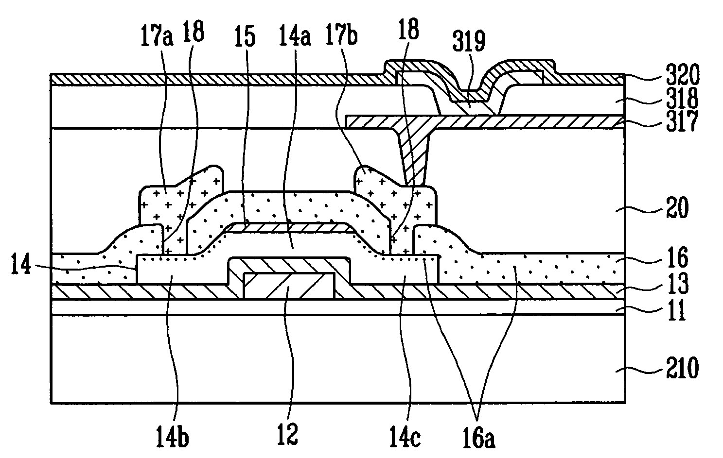
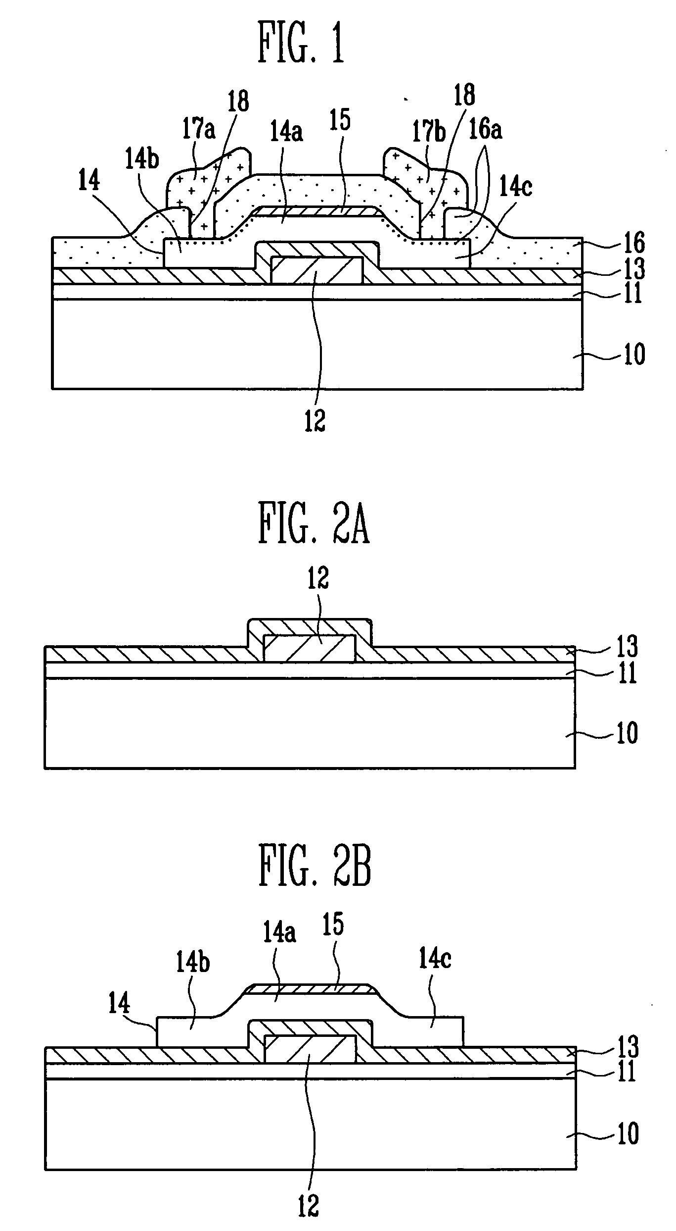
[0031]FIG. 1 illustrates a cross-sectional view of a TFT according to a Referring to FIG. 1, the TFT may be disposed on a substrate 10. The substrate 10 may have an insulating buffer layer 11 thereon. A gate electrode 12 may be on the buffer layer 11. A semiconductor layer 14 may extend across the gate electrode 12, the semiconductor layer 14 being insulated from the gate electrode 12 by a gate insulating layer 13. The semiconductor layer 14 may include a channel region 14a, a source region 14b, and a drain region 14c.

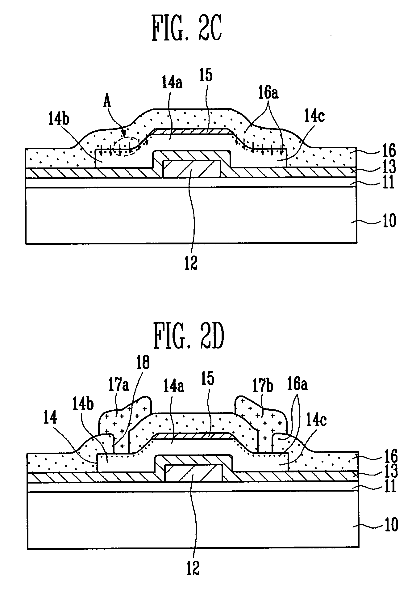
[0032]A hydrogen diffusion barrier layer 15 may be on the channel region 14a of the semiconductor layer 14. An interlayer dielectric layer 16 may extend across the hydrogen diffusion barrier layer 15 and the semiconductor layer 14. The hydrogen diffusion barrier layer 15 may cover the channel region 14a, such that the hydrogen diffusion barrier layer 15 is between the channel region 14a and the interlayer dielectric layer 16. The hydrogen diffusion barrier layer 15 m...

second embodiment

[0044]FIG. 3 illustrates a perspective view of a flat panel display device according to a The flat panel display device may include a display panel 100 for displaying images as a main element thereof. The display panel 100 may includes two substrates 110 and 120, and a liquid crystal layer 130. The two substrates 110 and 120 may be disposed opposite to each other, and the liquid crystal layer 130 may be interposed between the two substrates 110 and 120. A pixel region 113 may be defined by a plurality of gate lines 111 and a plurality of data lines 112, which may be arranged in a matrix. TFT's 114 and pixel electrodes 115 may be formed on the substrate 110 at the intersections of the gate lines 111 and the data lines 112. The TFT's 114 may controls signals supplied to respective pixels. The pixel electrodes 115 may be coupled to corresponding TFT's 114.

[0045]The TFT's 114 may be constructed as described above in connection with FIG. 1, and may be fabricated by the method described ...

third embodiment

[0047]FIG. 4A and FIG. 4B illustrate plan and cross-sectional views, respectively, of a flat panel display which includes a display panel 200 for displaying images as a main element. Referring to FIG. 4A, a substrate 210 may be have a pixel region 220 and a non-pixel region 230. The non-pixel region 230 may enclose, i.e., surround, the pixel region 220. A plurality of organic light emitting diodes (OLED's) 300 may be formed on the pixel region 220. The OLED's 300 may be coupled between scan lines 224 and data lines 226 in a matrix. Scan lines 224, data lines 226, and power supply lines (not shown) may be provided for operation of the OLED's 300. A scan driver 234 and a data driver 236 may be formed on the non-pixel region 230 of the substrate 210. The scan lines 224 and the data lines 226 may extend from the non-pixel region 230 to the pixel region 220. The scan driver 234 and the data driver 236 may process externally-provided signals, which may be provided via pads 228, and suppl...


PUM


Abstract

A thin film transistor includes a gate electrode, a first insulating layer on the gate electrode, a semiconductor layer on the gate electrode and separated from the gate electrode by the first insulating layer, the semiconductor layer including a channel region corresponding to the gate electrode, a source region, and a drain region, a hydrogen diffusion barrier layer on the semiconductor layer, the hydrogen diffusion barrier layer covering the channel region and exposing the source and drain regions, and a second insulation layer on the source and drain regions and on the hydrogen diffusion barrier layer, such that the hydrogen diffusion barrier layer is between the second insulation layer and the channel region.

Description

BACKGROUND OF THE INVENTION[0001]1. Field of the Invention[0002]Embodiments relate to a thin film transistor, a flat panel display device having the same, and associated methods.[0003]2. Description of the Related Art[0004]In general, a thin film transistor (“TFT”) includes a semiconductor layer and a gate electrode. The semiconductor layer includes a channel region, a source region, and a drain region. The gate electrode corresponds to the channel region of the semiconductor layer and is electrically insulated therefrom. The semiconductor layer may be formed of amorphous silicon or polysilicon. When the semiconductor layer is formed of amorphous silicon, the mobility may be low. Accordingly, it may be difficult to employ such TFT's in high speed circuits. In contrast, polysilicon may provide high mobility. The threshold voltage of TFT's formed from polysilicon may be non-uniform, however, and thus an additional compensating circuit may be required. Moreover, manufacturing a TFT usi...

Claims


Application Information

Patent Timeline
IPC IPC(8): H01L29/49G02F1/1368H01L21/28
CPCH01L29/66742H01L29/78606H01L29/7869H01L29/66969G02F2201/501G02F2202/10H01L27/12G02F1/1368H01L27/1225H01L29/78618H01L29/78636
Inventor SHIN, HYUN-SOOMO, YEON-GONJEONG, JAE-KYEONGPARK, JIN-SEONGLEE, HUN-JUNGJEONG, JONG-HAN
Owner SAMSUNG DISPLAY CO LTD
Why Eureka
Try Eureka