
Hydrogen sensor

a technology of hydrogen sensor and sensor, applied in the direction of gas analyser construction details, instruments, specific gravity measurement, etc., can solve the problems of lack of sensitivity, large power consumption, lack of sensitivity, etc., and achieve high electrical impedance, reduce this impedance, and large surface to volume ratio

Inactive Publication Date: 2011-08-09
UNIV OF SOUTH FLORIDA
View PDF5 Cites 0 Cited by
  • Summary
  • Abstract
  • Description
  • Claims
  • Application Information

AI Technical Summary

Benefits of technology

The present invention provides a hydrogen sensor with high sensitivity, fast regeneration, and a faster response time. The sensor has a low resistivity substrate and a hydrogen absorbing layer with nanoclusters that can adsorb up to 900 times its volume of hydrogen gas. The sensor can operate at room temperature and has a lower cost of production compared to previous sensors. The sensor can be easily integrated into sensor arrays or "system on a chip". The method of fabricating the sensor involves forming a nanoporous silicon substrate, depositing layers of palladium on the substrate, annealing the palladium layers, and diffusing the palladium into the nanoporous silicon to form nanoclusters of palladium oxide. The sensor responds to low concentrations of hydrogen in real time and has a high surface to volume ratio in the palladium nanoparticles, resulting in higher sensitivity, faster response, and shorter desorption times.

Problems solved by technology

These techniques generally either require a lot of power, show a slow response time or lack the required sensitivity.
However they lack the sensitivity needed and do not respond to low concentrations of hydrogen.
Additionally, the techniques used to fabricate these nanowire sensors require complex procedures, such as the transfer of nanostructures and their organized assembly.
These complex fabrication methodologies add to the cost of manufacture making nanowire sensors unsuitable for commercial production.
The increased number of conducting pathways results in an overall net decrease in resistance.

Method used


Image

  • Hydrogen sensor
  • Hydrogen sensor
  • Hydrogen sensor

Examples


Embodiment Construction

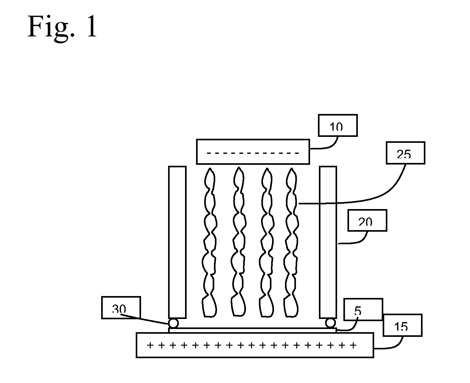
[0028]With reference to FIG. 1, in a particular embodiment, the porous silicon substrate 5 was fabricated from a p-type (1 0 0) silicon wafer of low resistivity (0.001-0.004Ω cm). The wafer 5 was anodized in an electrochemical etching solution 25 consisting of 24% HF / ethanol / H2O. The wafer 5 and platinum cathode 10 were placed in a Teflon jig, having sidewalls 20 and a rubber seal 30, as schematically illustrated in FIG. 1. The surfaces of the Si substrate 5 and Pt cathode 10 were kept parallel to each other and the current flow in the etchant 25 was normal to the wafer surface. The wafer 5 was etched at a current density of 25 mA / cm2 for an hour. The wafer was then removed from the etching bath, rinsed with water, and cleaned. This resulted in formation of an array of nanopores normal to the wafer, all being substantially parallel to each other.

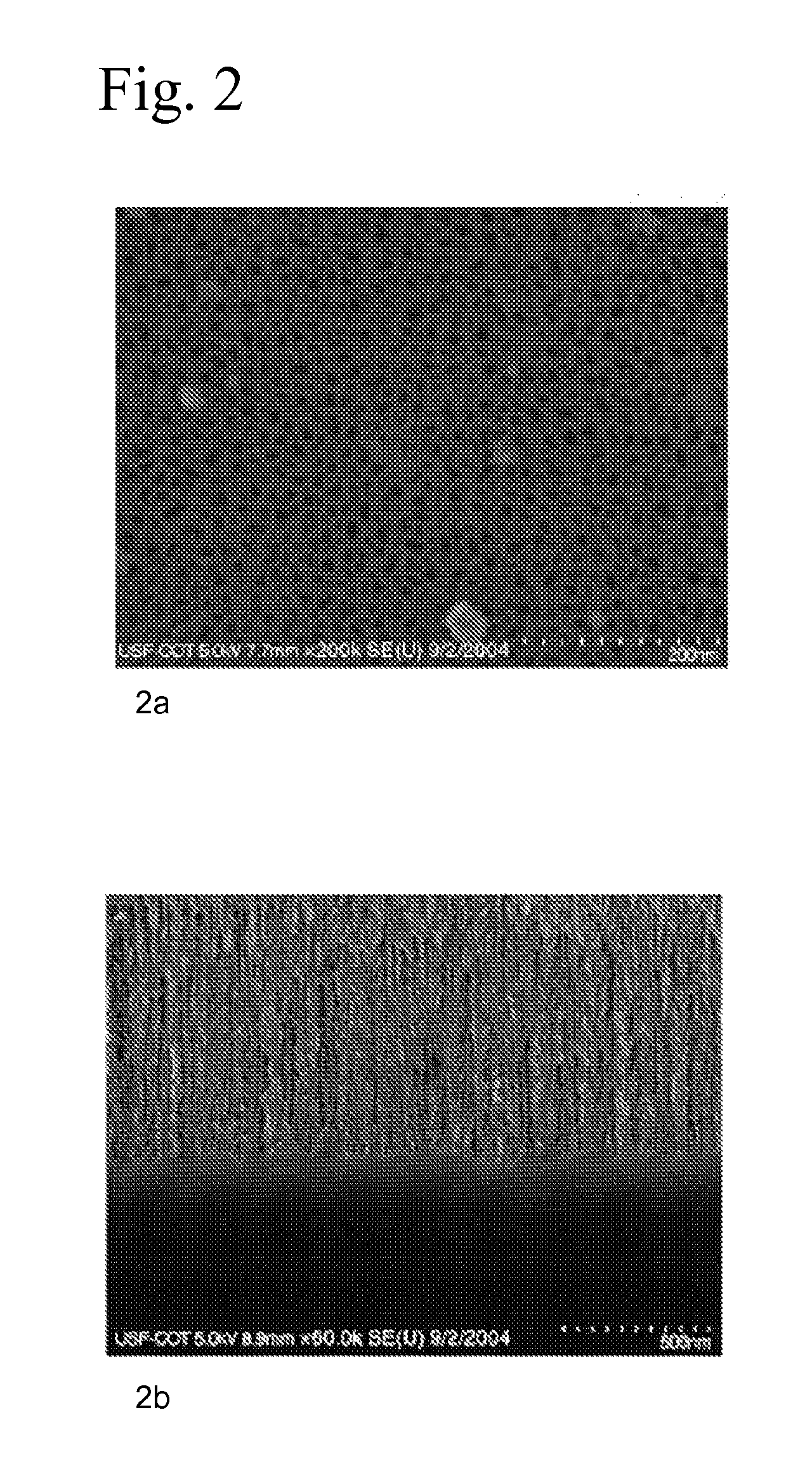
[0029]FIG. 2 shows the (a) surface and (b) cross-sectional Scanning Electron Micrograph (SEM) of the wafer following the porous Si etching ...


PUM

PropertyMeasurementUnit
diameteraaaaaaaaaa
diameteraaaaaaaaaa
thicknessaaaaaaaaaa

Abstract

A novel, resistance-based porous silicon sensor with Pd nano structures as the hydrogen sensing layer is presented. The sensor operates at room temperature. The hydrogen sensor of the present includes a p-Type Si substrate that is subjected to porous Si etching to form a nanoporous substrate. The substrate is then coated with a thin layer of Pd and annealed at 900 degrees C. This results in some Pd getting oxidized on porous Si and a thin PdO layer forms on the surface of the substrate. The sensor in accordance with the present invention exhibits an inverse relationship between increased hydrogen concentration versus resistance.

Description

CROSS REFERENCE TO RELATED APPLICATIONS[0001]This application claims priority to currently U.S. Provisional Patent Application 60 / 711,185, entitled, “High Sensitivity Hydrogen Sensor”, filed Aug. 25, 2005.STATEMENT OF GOVERNMENT INTEREST[0002]This invention was made with Government support under Grant No. 0403800 and 0239262 awarded by the National Science Foundation. The Government has certain rights in the invention.BACKGROUND OF THE INVENTION[0003]The need for a hydrogen sensor with high sensitivity, fast regeneration, and an even faster response time is gaining momentum as efforts to develop a hydrogen economy continue to grow. Numerous companies and organizations such as NASA and DOE, that use large quantities of hydrogen and oversee the development of the technology, have outlined a detailed performance criterion for an acceptable hydrogen sensor. Numerous approaches are being investigated to develop these hydrogen sensors, including sol-gel-based sensors, semiconductor sensor...

Claims


Application Information

Patent Timeline
Patent Type & Authority Patents(United States)
IPC IPC(8): G01N30/00G01N27/12
CPCG01N33/005Y10S977/957
Inventor LUONGO, KEVINBHANSALI, SHEKHAR
Owner UNIV OF SOUTH FLORIDA
Learn More