

Ceramic electronic component, circuit board arrangement, and method of manufacturing ceramic electronic component
a technology of ceramic electronic components and circuit boards, applied in the direction of fixed capacitor details, capacitors, fixed capacitors, etc., can solve the problem that certain types of elements cannot be effective in preventing
- Summary
- Abstract
- Description
- Claims
- Application Information
AI Technical Summary
Benefits of technology
Problems solved by technology
Method used
Image

Examples
first embodiment
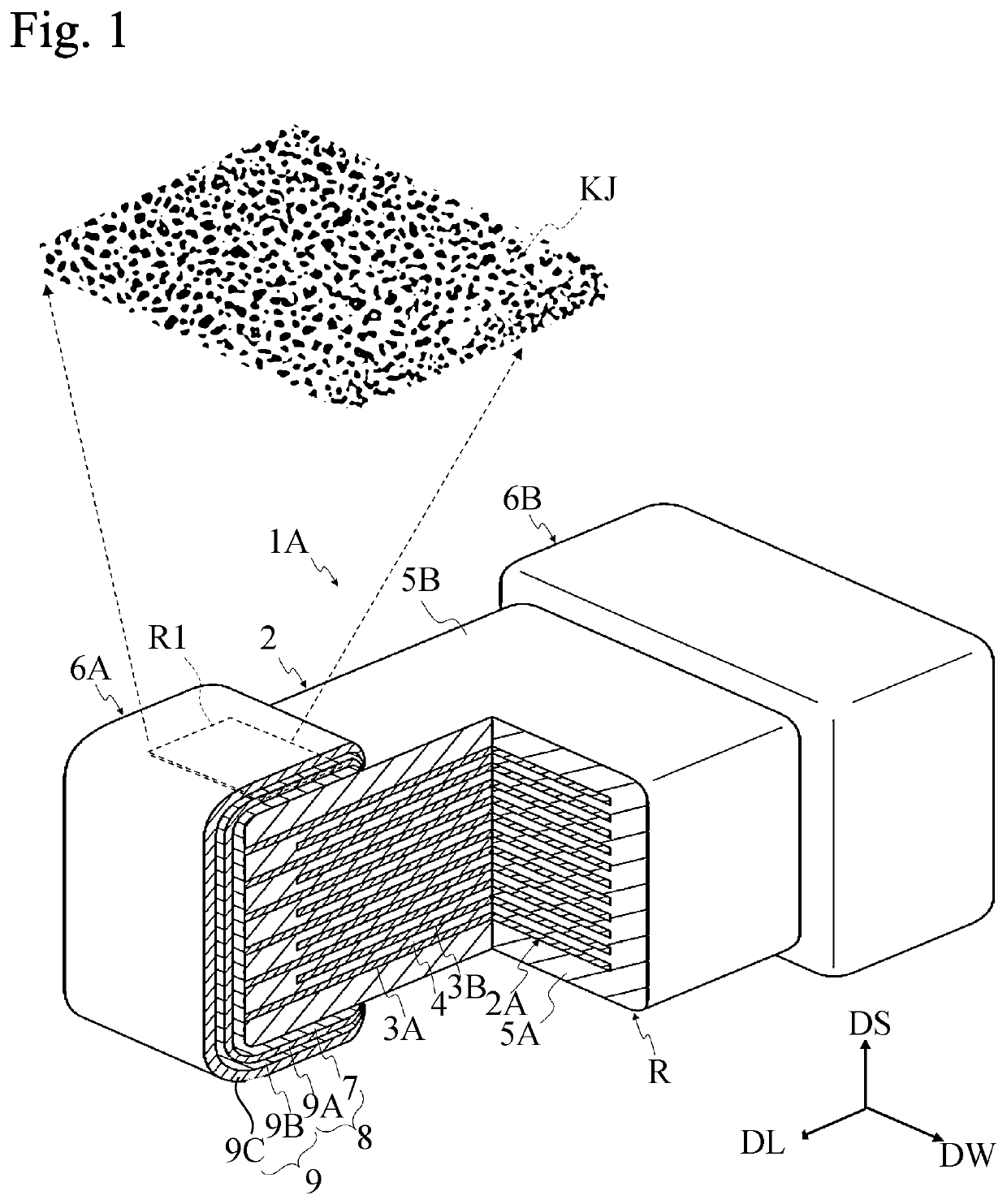
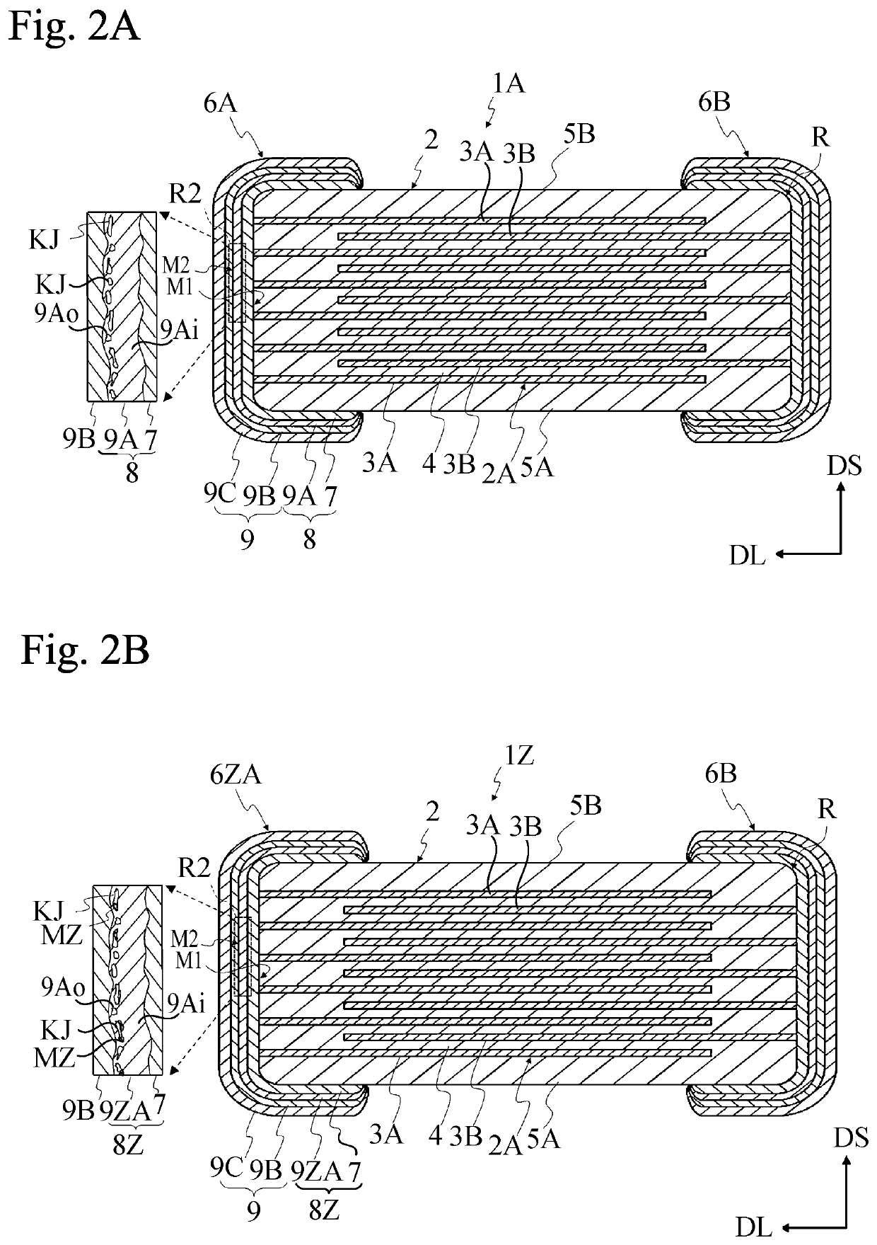
[0040]FIG. 1 is a perspective view showing a multilayer ceramic capacitor 1A according to a first embodiment of the present invention. FIG. 2A is a cross-sectional view of the multilayer ceramic capacitor 1A of FIG. 1 taken along the longitudinal direction thereof. In FIG. 1, an area R1 of an innermost plating layer 9A is shown in enlargement. In FIG. 2A, a cross sectional region R2 of an external electrode 6A is shown in enlargement. In this embodiment, a multilayer ceramic capacitor is taken as an example as a ceramic electronic component.
[0041]In FIGS. 1 and 2A, the multilayer ceramic capacitor 1A includes an element body (element assembly) 2 and external electrodes (outer electrodes) 6A and 6B. The element body 2 has a laminate (or stack) 2A, a lower cover layer 5A, and an upper cover layer 5B. The laminate 2A has internal electrode layers (inner electrode layers) 3A, other internal electrode layers 3B, and dielectric layers 4 interposed between neighboring internal electrode la...
second embodiment
[0095]FIG. 5 is a cross-sectional view showing a circuit board arrangement according to a second embodiment of the present invention, on which a multilayer ceramic capacitor is mounted. The circuit board arrangement includes a circuit board 11 and the multilayer ceramic capacitor 1A mounted on the circuit board 11.
[0096]As shown in FIG. 5, land electrodes 12A and 12B are formed on the circuit board 11. The circuit board 11 may be a printed circuit board or a semiconductor board formed from, for example, Si. The multilayer ceramic capacitor 1A is connected to the land electrodes 12A and 12B via solder layers 13A and 13B attached to the outermost plating layers 9C of the external electrodes 6A and 6B, respectively.
[0097]By providing voids KJ in the innermost plating layers 9A, stress exerted in the exterior electrodes 6A and 6B can be absorbed by the voids KJ. Therefore, when external stress is applied to the external electrodes 6A and 6B due to deflection or expansion and contraction...
third embodiment
[0098]FIG. 6 is a cross-sectional view showing a multilayer ceramic capacitor according to a third embodiment of the present invention taken along the longitudinal direction thereof. In FIG. 6, a cross sectional region R3 of an external electrode 6A′ is shown in enlargement.
[0099]In FIG. 6, the multilayer ceramic capacitor 1B has external electrodes 6A′ and 6B′ instead of the external electrodes 6A and 6B of FIG. 2A.
[0100]The external electrodes 6A′ and 6B′ are located on opposite sides of the element body 2, respectively, so that the external electrodes 6A′ and 6B′ are spaced apart (separated) from each other. Each of the external electrodes 6A′ and 6B′ continuously covers the top surface, the side surface, and the bottom surface of the element body 2. Each of the external electrodes 6A′ and 6B′ may also cover the front surface and the rear surface of the element body 2.
[0101]The external electrode 6A′ is connected to the internal electrode layers 3A, whereas the external electrode...
PUM
| Property | Measurement | Unit |
|---|---|---|
| thickness | aaaaa | aaaaa |
| length | aaaaa | aaaaa |
| thickness | aaaaa | aaaaa |
Abstract
Description
Claims
Application Information