Method for forming metal replacement gate of high performance

a metal replacement gate and high-performance technology, applied in the direction of semiconductor devices, basic electric elements, electrical appliances, etc., can solve the problems of incompatibility with high-k dielectric materials, less advantages of polysilicon gates over metal gates, and not nearly as good conductors as metal gates. achieve the effect of high-performance devices

Inactive Publication Date: 2005-07-26
GLOBALFOUNDRIES U S INC
View PDF15 Cites 143 Cited by
  • Summary
  • Abstract
  • Description
  • Claims
  • Application Information

AI Technical Summary

Problems solved by technology

However, as used in transistors, polysilicon gates are less advantages than metal gates.
Another disadvantage of polysilicon gates is its incompatibility with high-k dielectric materials.
Moreover, polysilicon, even when highly doped to dopant concentrations up to 1020cm −3, is not nearly as good a conductor as metal.
Manufacturing of metal gates, however, can pose serious challenges.
For one, metal gates are not thermally robust like polysilicon and therefore cannot be exposed to high temperatures during processing of transistors or other elements of integrated circuits (ICs).
Furthermore, metal gates cannot withstand the oxidation ambient necessary to form polysilicon transistor gates.
In addition, patterning accuracy required in gate formation is reduced when performing photolithography or other similar techniques on metal surfaces.
A particular challenge arises in the deposition of tungsten, however, especially when using WF6 as the deposition precursor.
Fluorine radicals in the WF6 gas can be harmful both to oxide and silicon substances.
In addition, the non-conformal property of such deposition causes tungsten to accumulate unevenly so that a void is created in the middle or center of the tungsten gate, rendering the gate structurally defective.
The pinchoff problem is extremely challenging in high performance environments where the width of the opening is narrow.
Another challenge, when using either WF6 or W(CO)6 gases, is that effective deposition of tungsten requires a good nucleation site to be present on the surfaces (i.e. sidewalls) where it is being deposited.
Ineffective deposition of tungsten can lead to structurally defective gates in which the gate conductor material may peel or pop off from their adjacent surfaces.

Method used


Image

  • Method for forming metal replacement gate of high performance
  • Method for forming metal replacement gate of high performance
  • Method for forming metal replacement gate of high performance

Examples


Embodiment Construction

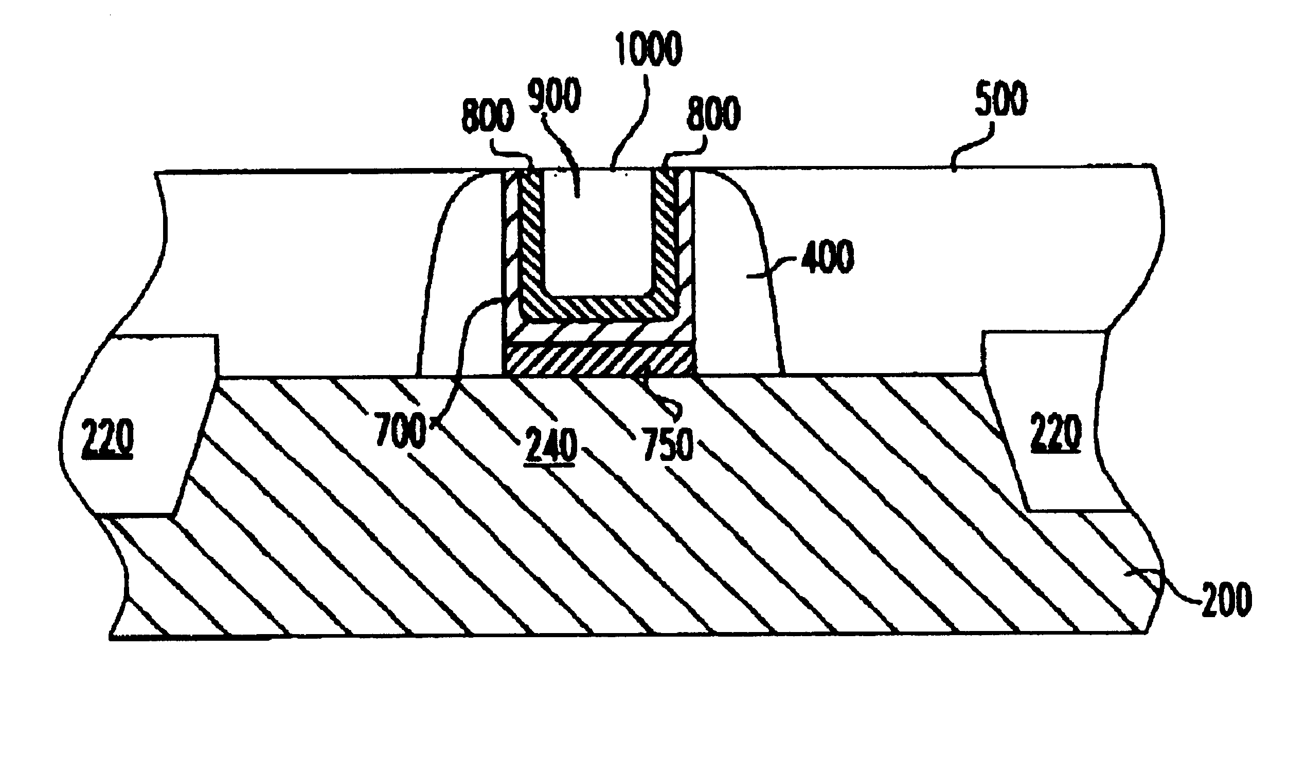
[0020]The present invention particularly addresses and solves problems related to the formation of metal gates in transistors. In an embodiment of the invention, the metal can be selected for workfunction compatibility with the conductivity type of transistor in which it is used. For example, in an NFET, a metal gate having a workfunction equivalent to that of n-type conductivity semiconductor material performs better than a metal having a mid-range workfunction or a workfunction equivalent to that of p-type semiconductor material. In an embodiment of the invention, a structure and method are provided by which a metal having a desirable workfunction can be formed in contact with the gate dielectric in an integrated structure and method that decouples the particular choice of metal used in that step from later processing.

[0021]In an embodiment described herein, the particular metal formed in contact with the gate can be selected for its compatibility with the gate dielectric material...


PUM

PropertyMeasurementUnit
thickaaaaaaaaaa
thickaaaaaaaaaa
temperatureaaaaaaaaaa

Abstract

A structure and method for a metal replacement gate of a high performance device is provided. A sacrificial gate structure is first formed on an etch stop layer provided on a semiconductor substrate. A pair of spacers is provided on sidewalls of the sacrificial gate structure. The sacrificial gate structure is then removed, forming an opening. Subsequently, a metal gate including an first layer of metal such as tungsten, a diffusion barrier such as titanium nitride, and a second layer of metal such as tungsten is formed in the opening between the spacers.

Description

BACKGROUND OF INVENTION[0001]The invention relates to a semiconductor structure and processing method, and more particularly to an improved structure and method for a metal gate structure of a high performance device.[0002]In the semiconductor fabrication industry, transistors have typically been formed utilizing polysilicon gate electrodes. Polysilicon has been preferred because of its thermal robustness and other special characteristics. An important feature of polysilicon gates is that they can withstand the processing of other elements of transistors such as source and drain regions, during dopant drive-in or other high temperature processes such as annealing processes.[0003]However, as used in transistors, polysilicon gates are less advantages than metal gates. A polysilicon gate is subject to the formation of a depletion region in operation in which charge carriers are depleted from the polysilicon material above the gate dielectric. This varies from a metal electrode in which...

Claims


Application Information

Patent Timeline
Patent Type & Authority Patents(United States)
IPC IPC(8): H01L21/28H01L21/336H01L21/02H01L29/49H01L29/40
CPCH01L21/28079H01L29/4958H01L29/66545H01L21/18
Inventor CABRAL, JR., CYRILJAMISON, PAUL C.KU, VICTORLI, YINGNARAYANAN, VIJAYSTEEGEN, AN LWANG, YUN-YUWONG, KWONG H.
Owner GLOBALFOUNDRIES U S INC
Why Eureka
Try Eureka