Phase change tip storage cell

a technology of phase change and storage cells, applied in the field of solid-state storage, can solve the problems of increasing the cost of reducing the contact area normally, reducing the contact area, so as to reduce the power required

Active Publication Date: 2005-06-16
GLOBALFOUNDRIES US INC
View PDF6 Cites 143 Cited by
  • Summary
  • Abstract
  • Description
  • Claims
  • Application Information

AI Technical Summary

Benefits of technology

[0012] It is yet another purpose of the invention to reduce the power required to deliver sufficient heat to set and reset phase change material in individual memory cells.

Problems solved by technology

Unfortunately, a relatively of large current is needed for each memory element to heat the phase change material.
In particular, resetting the phase change material may require heating the crystalline material to its melting point, generally above 600° C. Thus, it maybe difficult on one hand to provide sufficient localized heat to raise the crystalline phase change material to its melting point and, on the other hand, to avoid accidentally heating other adjacent cells to the phase change set point and inadvertently setting adjacent cells.
Unfortunately, reducing the contact area normally increases cost, which is inversely proportional to the size of the contact.
In particular, attaining a contact size below the minimum photolithographic image size for a particular technology complicates the process significantly and, correspondingly, increases cost.
Further, normally, reducing contact size, reduces the heat delivery capability and increases resistance / reduces current delivered to the phase change material; all of which interferes with setting / resetting the material rather than enhancing it.

Method used


Image

  • Phase change tip storage cell
  • Phase change tip storage cell
  • Phase change tip storage cell

Examples


Embodiment Construction

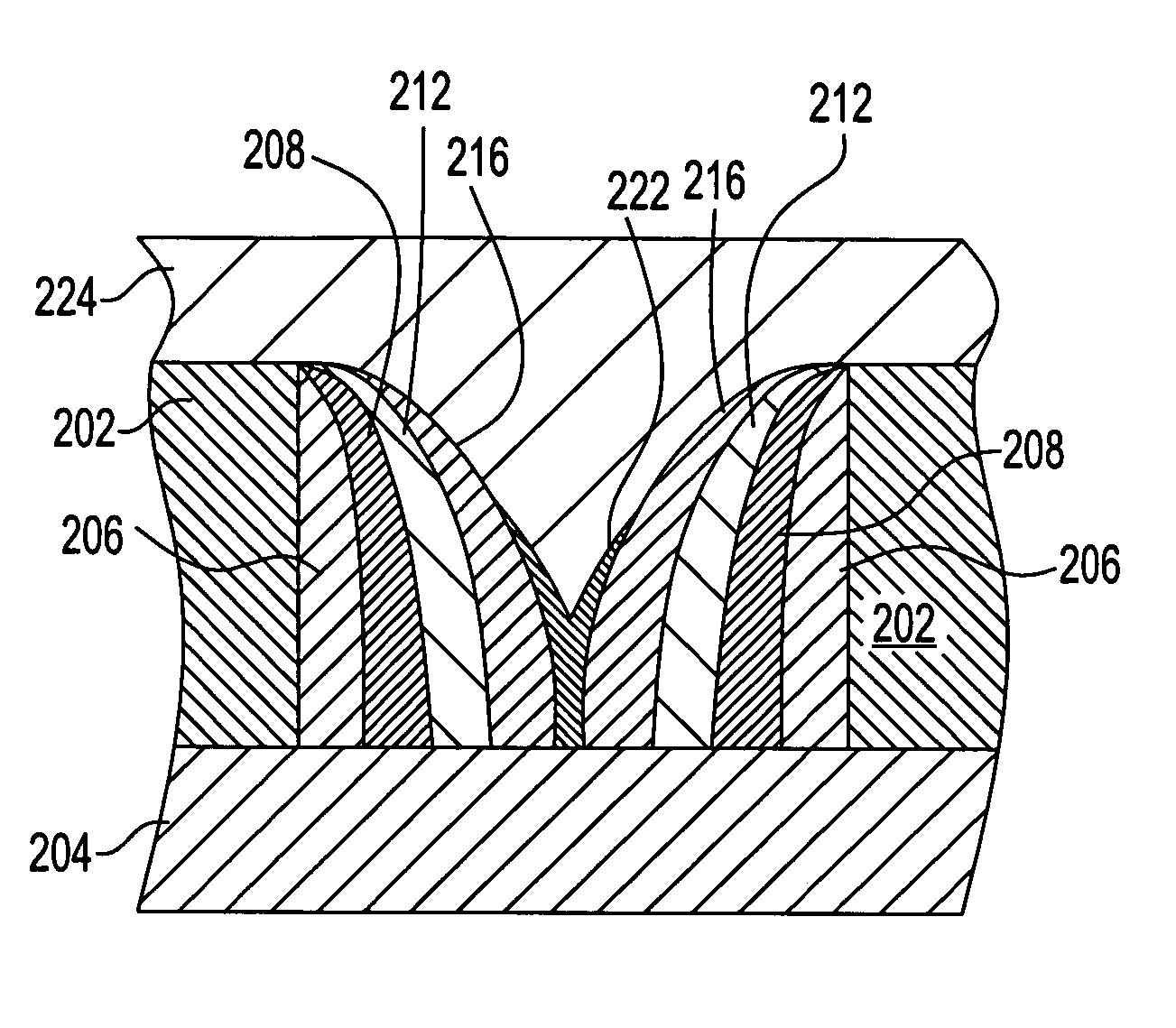
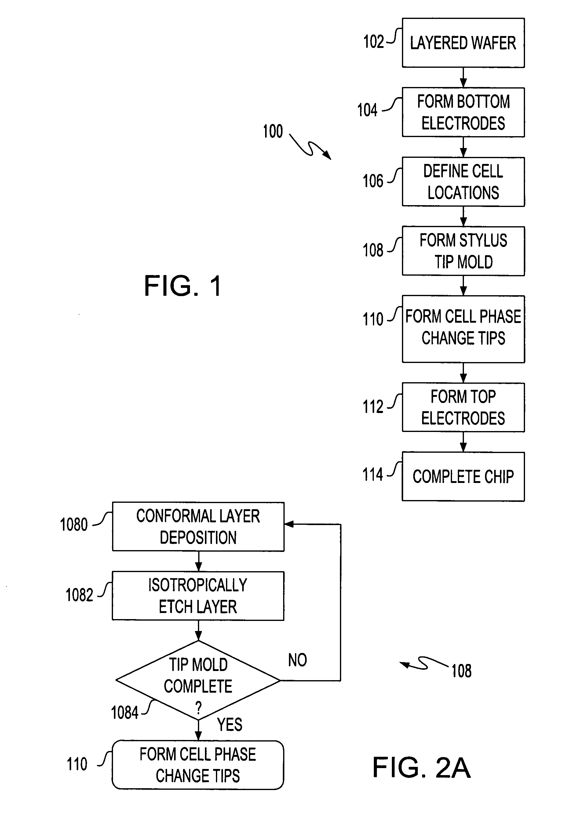
[0022] Turning now to the drawings and more particularly, FIG. 1 shows a flow diagram for an example of a method 100 of forming preferred embodiment nonvolatile storage devices according to the present invention, e.g., in a cross point storage array. In particular, preferred embodiment devices have chalcogenide phase change storage media in a stylus tip with a focused heating field in the stylus for enhanced Joule heating power delivery that improves phase change alteration. Preferably, Joule heating delivery is enhanced by delivering heat through and to the phase change material in the tip or apex of the stylus. In particular during a write, the hottest stylus region is spaced away from the bulk of the stylus and at the apex and so, contained entirely within the phase change material.

[0023] Cell formation begins in step 102 with a layered wafer. In particular, the layered wafer may be a partially patterned integrated circuit with standard insulated gate field effect transistor (FE...


PUM

PropertyMeasurementUnit
melting pointaaaaaaaaaa
pressureaaaaaaaaaa
temperatureaaaaaaaaaa

Abstract

A storage cell, integrated circuit (IC) chip with one or more storage cells that may be in an array of the storage cells and a method of forming the storage cell and IC. Each storage cell includes a stylus, the tip of which is phase change material. The phase change tip may be sandwiched between an electrode and conductive material, e.g., titanium nitride (TiN), tantalum nitride (TaN) or n-type semiconductor. The phase change layer may be a chalcogenide and in particular a germanium (Ge), antimony (Sb), tellurium (Te) (GST) layer.

Description

CROSS REFERENCE TO RELATED APPLICATION [0001] The present invention is related to U.S. application Ser. No. ______ (Attorney Docket No. YOR920030482US1) entitled “FIELD EMISSION PHASE CHANGE DIODE STORAGE ELEMENT AND MEMORY” to Stephen S. Furkay et al. and U.S. application Ser. No. ______ (Attorney Docket No. YOR920030483US1) entitled “INTEGRATED CIRCUIT WITH UPSTANDING STYLUS” to David V. Horak et al., both filed coincident herewith and assigned to the assignee of the present invention.BACKGROUND OF THE INVENTION [0002] 1. Field of the Invention [0003] The present invention is related to solid state storage and particularly to solid state storage cells with a phase change material memory element. [0004] 2. Background Description [0005] Solid state, phase change materials that are chalcogen (Group VI elements such as sulfur (S), selenium (Se) and tellurium (Te)) alloys with at least one of germanium (Ge), arsenic (As), silicon (Si) and antimony (Sb) are known as chalcogenides and ar...

Claims


Application Information

Patent Timeline
Patent Type & Authority Applications(United States)
IPC IPC(8): G11C11/56G11C13/00H01L27/10H01L27/24H01L29/04H01L45/00
CPCH01L45/06H01L45/1233H01L27/2463H01L45/144H01L45/1691H01L45/1273H10B63/80H10N70/231H10N70/8418H10N70/826H10N70/8828H10N70/068
Inventor HORAK, DAVID V.LAM, CHUNG H.WONG, HON-SUM P.
Owner GLOBALFOUNDRIES US INC
Why Eureka
Try Eureka