IC device including package structure and method of forming the same

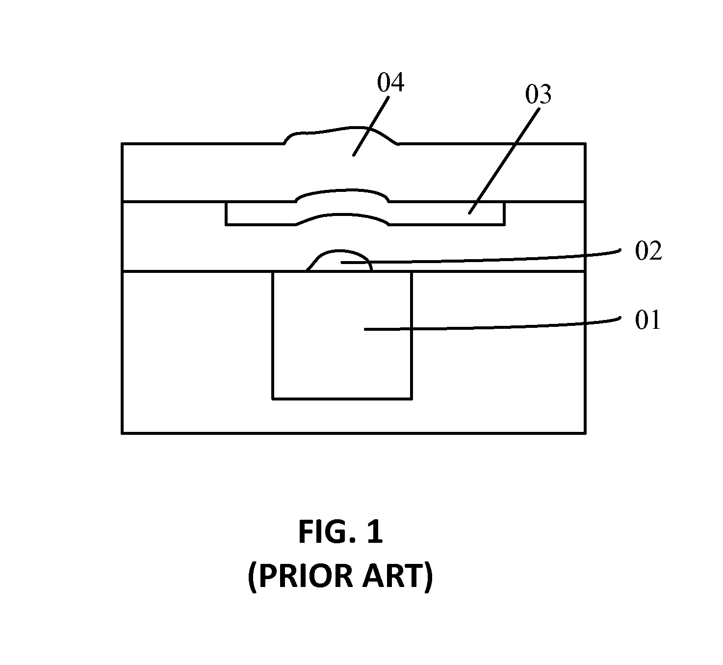
a technology of a package structure and a method of forming the same, which is applied in the direction of semiconductor devices, semiconductor/solid-state device details, electrical apparatus, etc., can solve the problems of increasing the difficulty of increasing the number of semiconductor devices in a two-dimensional (2d) package structure, mismatched thermal expansion of materials involved including copper, silicon and silicon oxide, and insufficient through-hole volume to accommodate thermal expansion of tsv copper

Active Publication Date: 2014-01-16
SEMICON MFG INT (SHANGHAI) CORP
View PDF5 Cites 135 Cited by
  • Summary
  • Abstract
  • Description
  • Claims
  • Application Information

AI Technical Summary

Benefits of technology

[0008]According to various embodiments, there is provided an integrated circuit (IC) device. The IC device can include a first metal interconnect structure disposed on a first substrate structure, and a second substrate structure disposed over the first substrate structure such that a through-hole in the second substrate structure is positioned over the first metal interconnect structure on the first substrate structure. The IC device can also include a second metal interconnect structure disposed on the second substrate structure, and an insulating layer disposed on sidewall of the through-hol

Problems solved by technology

Also, it has become increasingly difficult to increase the number of semiconductor devices in a two-dimensional (2D) package structure.
Under this high temperature, due to different thermal expansion coefficients, mismatched thermal expansion may occur to the materials involved including copper, silicon, and silicon oxide.
At high temperatures, the volume increase of the through-hole is not sufficient to accommodate thermal expansion of the TSV copper.
Consequently, copper may be extruded from the TSV top surface, which affects yield and reliability of the the

Method used


Image

  • IC device including package structure and method of forming the same
  • IC device including package structure and method of forming the same
  • IC device including package structure and method of forming the same

Examples


Embodiment Construction

[0015]Reference will now be made in detail to exemplary embodiments of the disclosure, which are illustrated in the accompanying drawings. Wherever possible, the same reference numbers will be used throughout the drawings to refer to the same or like parts.

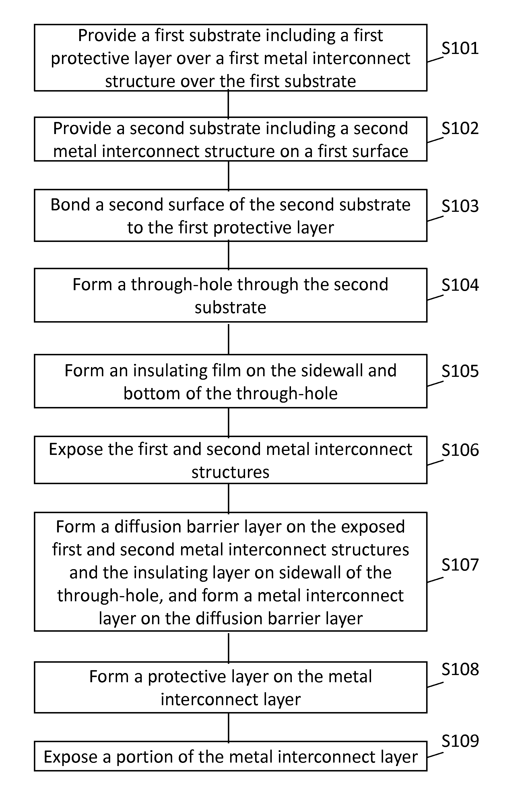
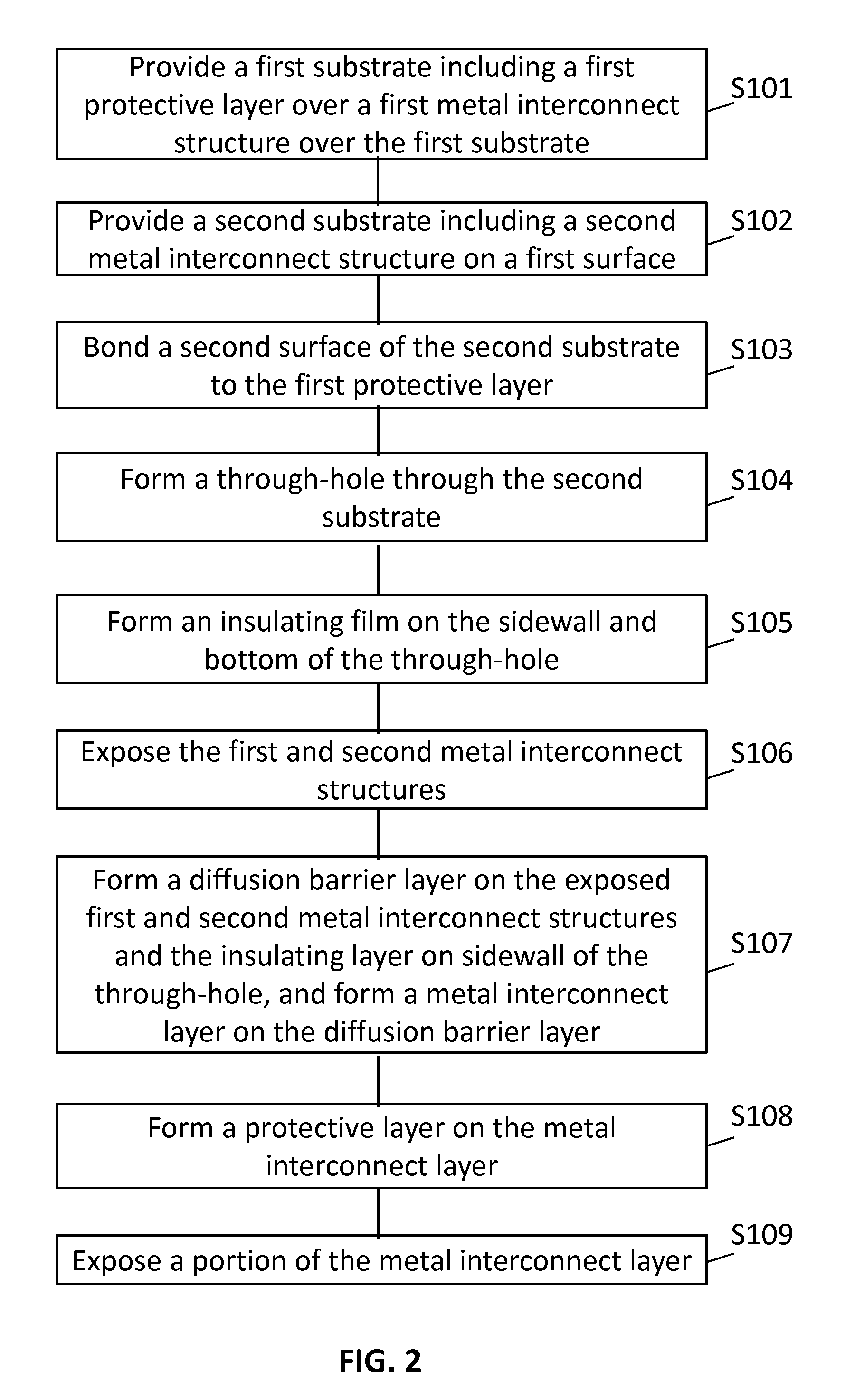
[0016]Various embodiments provide IC devices having a package structure and methods of forming the IC device. Generally, a through-silicon via (TSV) is known as a vertical electrical connection passing through a silicon wafer or die. As explained above, conventional TSVs include a copper pillar. As disclosed herein, a through-hole can be formed in a bonded structure and at least partially filled by one or more layers of material(s) to form an electrical interconnect between semiconductor devices in the bonded structure and thus to form a desired package structure. The material(s) filled in the through-hole do not include a copper pillar as known in the art.

[0017]In one embodiment, the through-hole can be filled with, e.g., an insu...


PUM


Abstract

Various embodiments provide semiconductor devices including a package structure and methods of forming the semiconductor devices. In one embodiment, the package structure can include a through-hole at least partially filled by one or more layers of material(s) to form a through-hole interconnect between semiconductor devices in the package structure. The through-hole can be filled by an insulating layer, a diffusion barrier layer, a metal interconnect layer, and/or a protective layer having a total thickness from the sidewall of the through-hole of less than or equal to the radius of the through-hole.

Description

CROSS-REFERENCES TO RELATED APPLICATIONS[0001]This application claims priority to Chinese Patent Application No. CN201210241511.3, filed on Jul. 12, 2012, the entire contents of which are incorporated herein by reference.FIELD OF THE DISCLOSURE[0002]The present disclosure relates to the field of semiconductor technology and, more particularly, relates to an IC device including a package structure and method of forming the same.BACKGROUND[0003]With development of semiconductor technology, the feature size of semiconductor devices in integrated circuit (IC) devices has been reduced. Also, it has become increasingly difficult to increase the number of semiconductor devices in a two-dimensional (2D) package structure. Three-dimensional (3D) packaging becomes an effective tool to improve integration degree of IC devices or chips. The 3D packaging methods may include die stacking and package stacking based on gold wire bonding, and 3D stacking based on through-silicon vias (TSVs). The TSV...

Claims


Application Information

Patent Timeline
IPC IPC(8): H01L23/52H01L21/768
CPCH01L23/52H01L21/76829H01L23/481H01L25/0657H01L2924/0002H01L21/76898H01L2225/06541H01L2924/00
Inventor GAN, ZHENGHAOCHEN, FANG
Owner SEMICON MFG INT (SHANGHAI) CORP
Why Eureka
Try Eureka