Method for manufacturing element isolation structural section

a technology of structural section and element, which is applied in the direction of semiconductor/solid-state device manufacturing, basic electric elements, electric apparatus, etc., can solve the problems of reducing the electrical characteristic of each element, and affecting the uniformity of the in-plane. achieve the effect of preventing the occurrence of divots and satisfying the uniformity

Inactive Publication Date: 2006-12-21
LAPIS SEMICON CO LTD
View PDF5 Cites 4 Cited by
  • Summary
  • Abstract
  • Description
  • Claims
  • Application Information

AI Technical Summary

Benefits of technology

[0021] According to the method for manufacturing the element isolation structural section, i.e., the STI, according to the present invention, for example, an HfSiON film corresponding to a film changed in etching rate by heat treatment is used as an alternative to a conventional so-called pad oxide film. By adjusting a temperature in a heating processing step, the HfSiON film is capable of adjusting its etching rate with hydrofluoric acid (HF) as an etchant. Thus, since the etching rate of the HfSiON film can be made larger than that of other film etched simultaneously, i.e., a precursor embedded oxide film, an excessive F / A (Field / Active) step subsequent to the removal of the HfSiON film leading up to the occurrence of divots can be made in a simpler process step and lower. Consequently, it is possible to ensure satisfactory in-plane uniformity while effectively preventing the occurrence of the divots. Thus, the electrical characteristics of elements separated by the STI can be prevented from degradation.
[0022] According to the STI manufacturing method of the present invention as well, since satisfactory in-plane uniformity can be realized, the present method can adapt even to further miniaturization of a manufacturing process.

Problems solved by technology

With developments in a semiconductor micro-fabrication technique, an element isolation method using a conventional LOCOS method is encountering difficulties in building element forming regions (hereinafter also called simply “active regions”) with elements formed therein in thin widths and with satisfactory accuracy.
In doing so, there is a fear that the electrical characteristic of an element formed in each active region is degraded.
There is however a fear that due to the overetching, for example, a gate oxide film formed in active region is damaged and the electrical characteristic of each element is degraded.
Thus, there is a fear that the above problems associated with the divots cannot be resolved even depending on such a manufacturing process.
A problem also arises in that the manufacturing process is complex and the number of manufacturing steps increases.

Method used


Image

  • Method for manufacturing element isolation structural section
  • Method for manufacturing element isolation structural section
  • Method for manufacturing element isolation structural section

Examples


Embodiment Construction

[0029] Preferred embodiments of the present invention will hereinafter be described with reference to the accompanying drawings. Incidentally, the shape, size and physical relationship of each constituent element or component in the figures are merely approximate illustrations to enable an understanding of the present invention. Therefore, the present invention is not limited only to examples illustrated in particular.

[0030] Although the specific materials, conditions and numerical conditions or the like might be used in the following description, they are no more than one of preferred examples. Accordingly, the present invention is by no means limited to these preferred examples.

[0031] Further, be cognizant of the fact that similar constituent elements illustrated in the respective figures used in the following description are given the same reference numerals, and their dual explanations might be omitted.

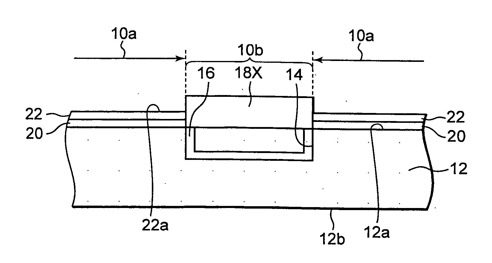
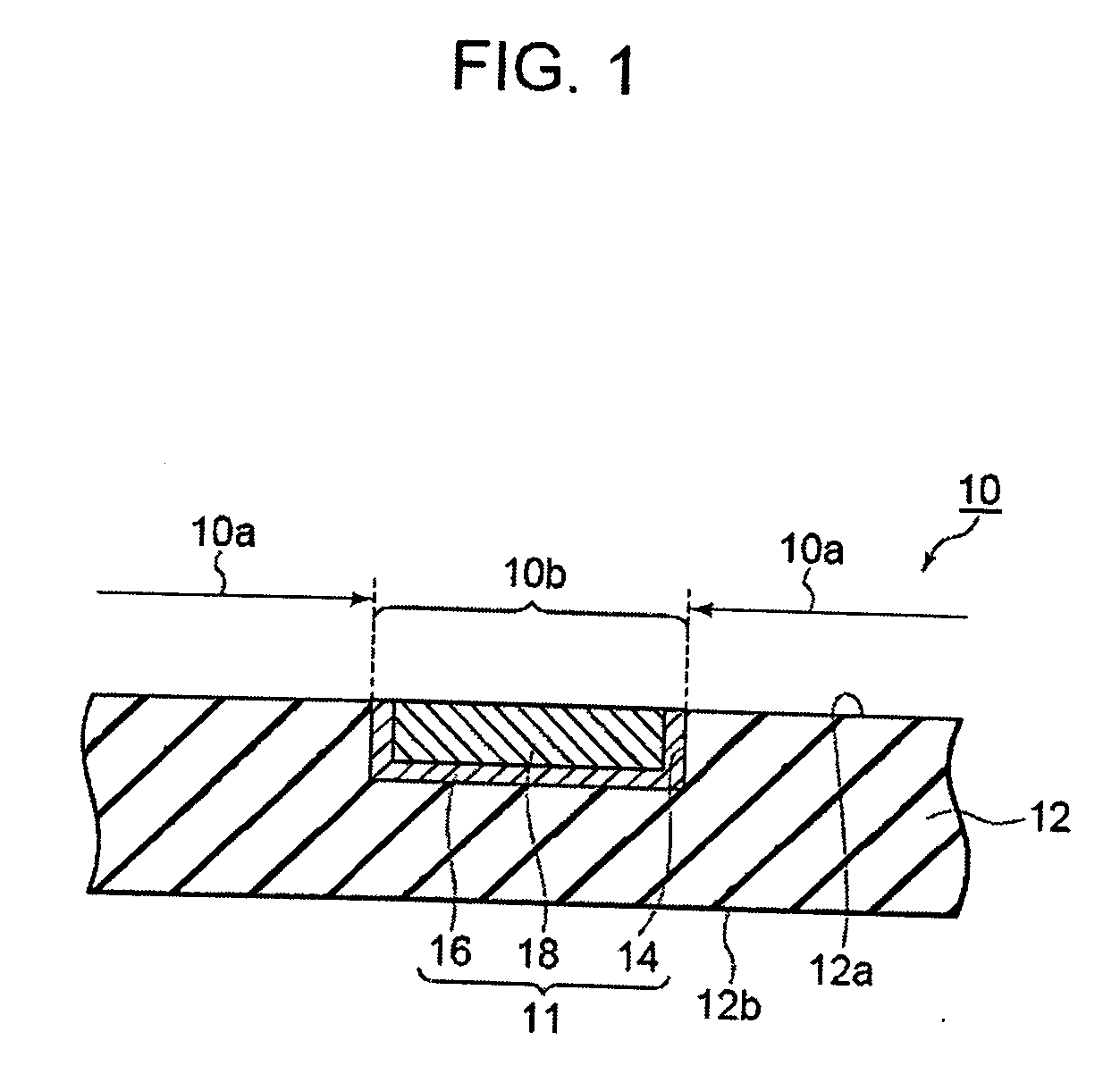
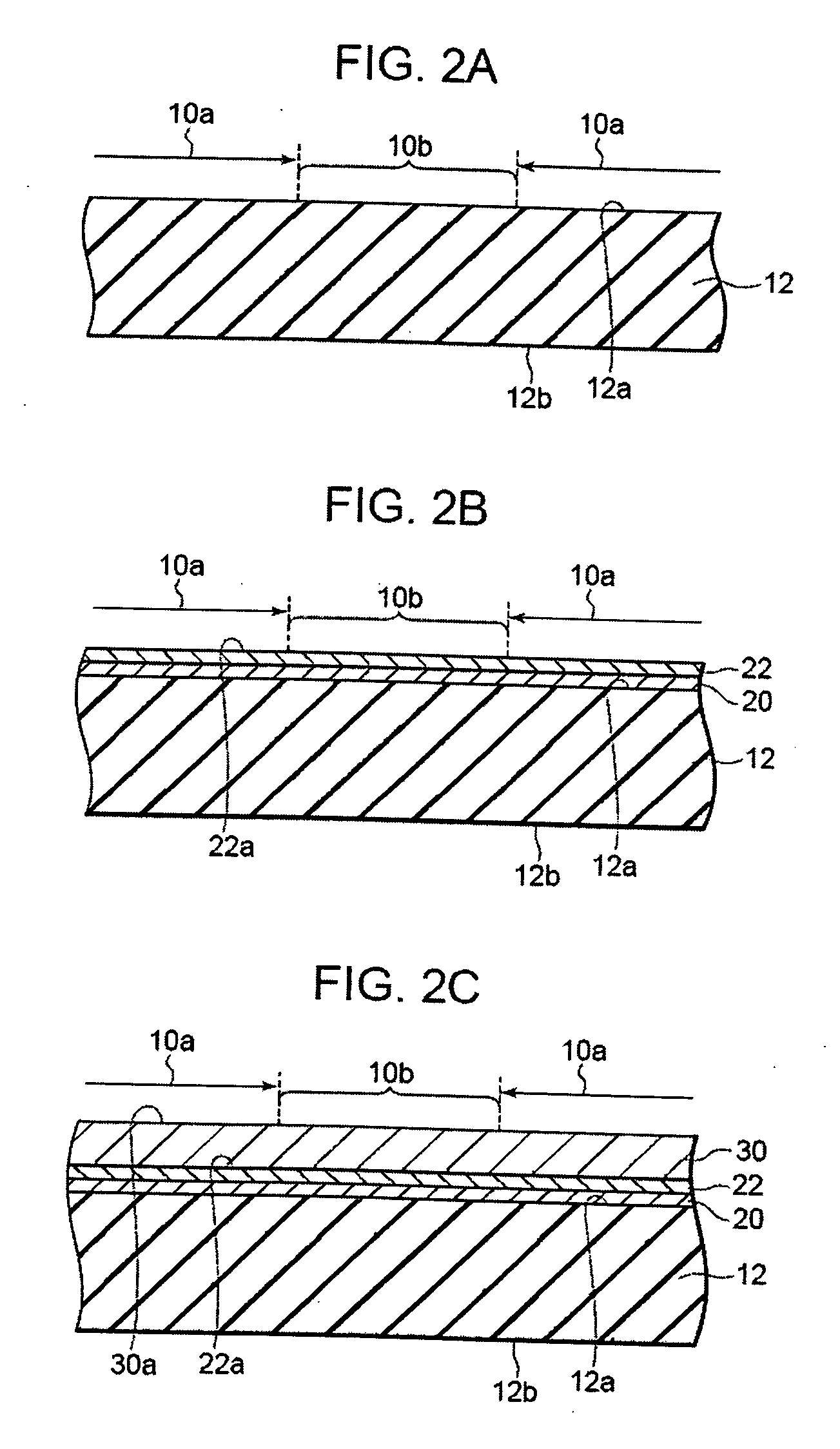
[0032] (Configuration of Element Isolation Structural Section)

[0033] A co...


PUM


Abstract

A plurality of element forming regions and an element isolation structural section forming region which separates the plurality of element forming regions from one another, are set to a substrate. A first thermal oxide film is formed. An HfSiON film is formed. Heating processing is done. A silicon nitride film is formed. A trench is formed which extends from an upper surface of the substrate, corresponding to the element isolation structural section forming region to within the substrate. A trench oxide film is formed. A precursor embedded oxide film is formed. The precursor embedded oxide film is removed as a height lower than the upper surface of the silicon nitride film. Then, the silicon nitride film is removed. The HfSiON film and the first thermal oxide film are removed. A second thermal oxide film is formed on an exposed surface of the substrate from which the HfSiON film and the first thermal oxide film are removed. An embedded portion is formed as the same height as that of the exposed surface of the substrate.

Description

BACKGROUND OF THE INVENTION [0001] The present invention relates to a method for manufacturing an element isolation structural section, particularly, a so-called Shallow Trench Isolation (hereinafter called simply “STI”) which separates a plurality of elements built in a semiconductor substrate from one another. [0002] With developments in a semiconductor micro-fabrication technique, an element isolation method using a conventional LOCOS method is encountering difficulties in building element forming regions (hereinafter also called simply “active regions”) with elements formed therein in thin widths and with satisfactory accuracy. In order to resolve such a problem, a shallow trench has been formed in a semiconductor substrate and element isolation based on an STI with the trench buried by a silicon oxide film has been carried out. [0003] In a film structure removal process employed in an STI manufacturing method, however, a wet etching step has often been performed in general. Due...

Claims


Application Information

Patent Timeline
Patent Type & Authority Applications(United States)
IPC IPC(8): H01L21/76
CPCH01L21/76224
Inventor ILNUMA, TAIKAN
Owner LAPIS SEMICON CO LTD
Why Eureka
Try Eureka