
Atomic layer deposition of thin films on germanium

a germanium substrate and thin film technology, applied in chemical vapor deposition coatings, electrical equipment, coatings, etc., can solve the problems of poor electrical properties, poor deposition effect, and inability to obtain films with good electrical properties, so as to facilitate ald on ge and facilitate subsequent deposition

Active Publication Date: 2006-12-28
ASM INTERNATIONAL
View PDF20 Cites 47 Cited by
  • Summary
  • Abstract
  • Description
  • Claims
  • Application Information

AI Technical Summary

Benefits of technology

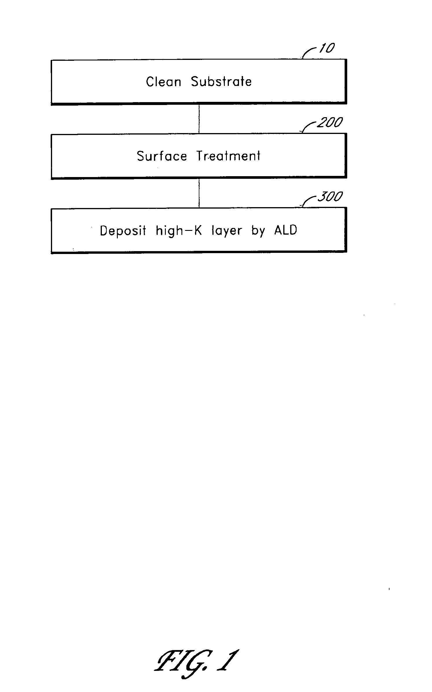
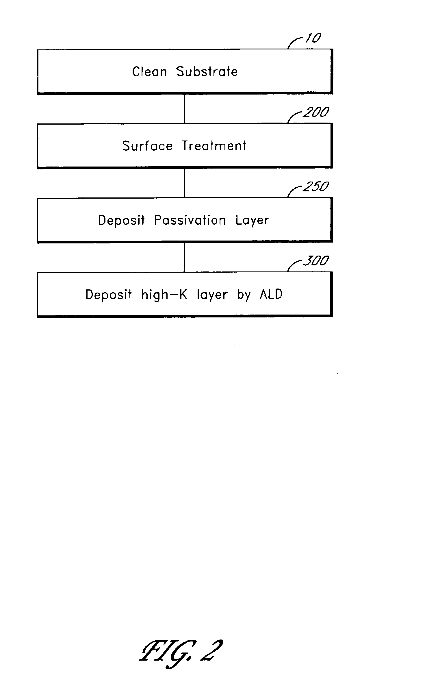
[0010] Methods for depositing thin films, such as high-k dielectric layers, on Ge substrates by atomic layer deposition (ALD) are provided. The surface of the Ge substrate is preferably cleaned and / or treated to provide a uniform surface termination that facilitates subsequent deposition of a thin film by ALD. In some embodiments the treatment includes the formation of an ultra-thin layer of GeOx or GeOxNy. The surface treatment may also include etching of native oxide.
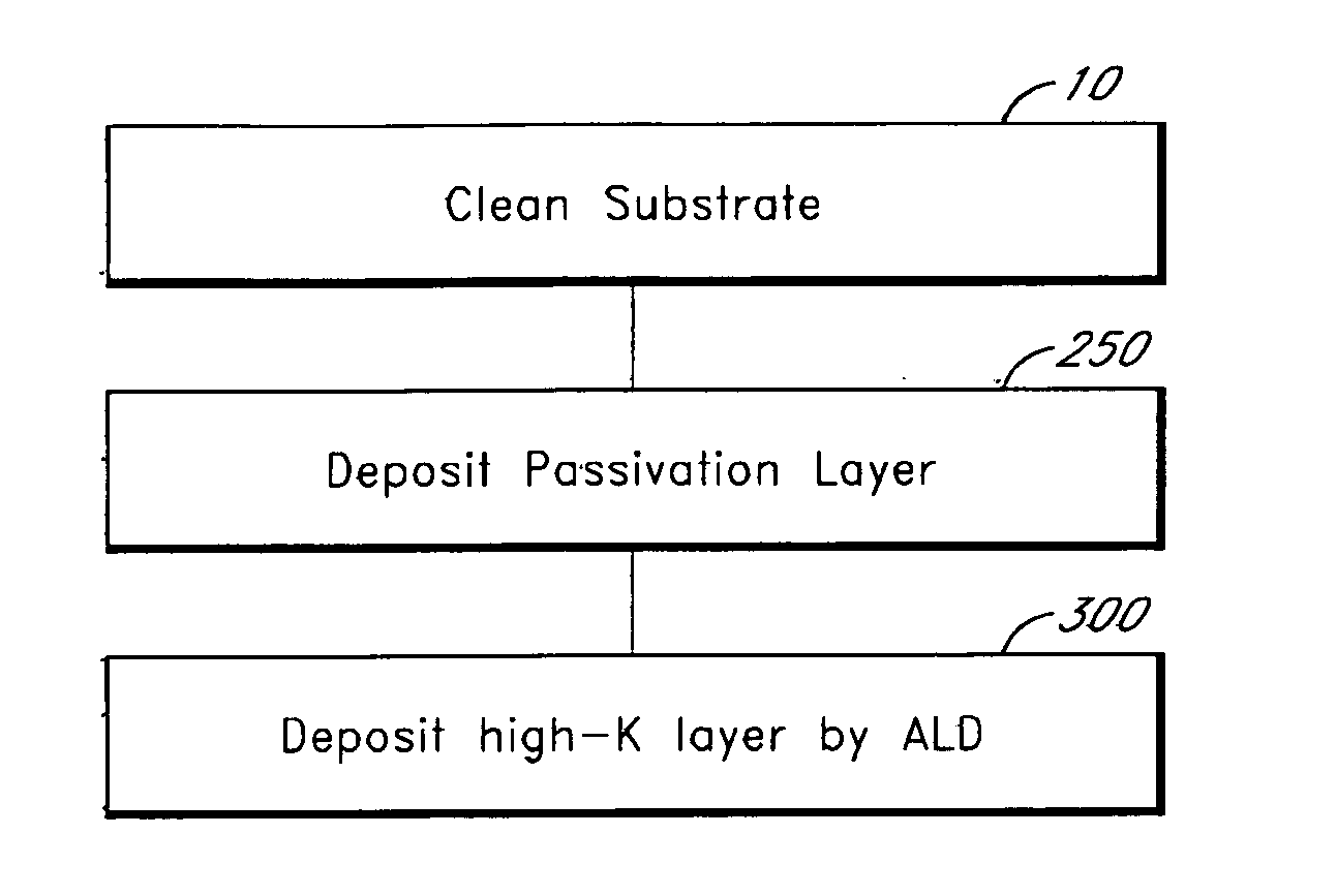
[0011] In some embodiments, a passivation layer is also used to facilitate ALD on Ge. For example, a thin metal oxide layer may be deposited over the substrate surface prior to deposition of a thin film by ALD. In preferred embodiments, surface treatment, such as the formation of GeOx or GeOxNy and / or etching of native oxide, is combined with deposition of a passivation layer.
[0012] Following surface treatment and / or deposition of a passivation layer, a thin film is deposited over the substrate by ALD. In some embodiments the ALD process uses a metalorganic reactant and is carried out at a temperature of less than about 300° C.

Problems solved by technology

The tradeoff, however, is much decreased mobility.
However, because germanium does not have a stable native oxide like silicon, it has not been possible to obtain films with good electrical properties.
The instability of germanium oxides explains the poor electrical properties obtained so far.

Method used


Image

  • Atomic layer deposition of thin films on germanium
  • Atomic layer deposition of thin films on germanium
  • Atomic layer deposition of thin films on germanium

Examples


Embodiment Construction

[0016] Thin films, such as high-k dielectric layers, can be deposited on Ge substrates by ALD. However, as discussed above, native germanium oxide is not stable. Thus, in order to ensure that the deposited films have good physical and electrical properties a surface termination that provides good reactive sites for ALD growth should be maintained or provided. A number of approaches for facilitating ALD growth on germanium substrates have been identified.

[0017] According to one aspect of the invention the surface of the germanium substrate is treated to provide good reactive sites for ALD growth. The surface treatment preferably provides a uniform distribution of a surface termination, such as hydroxyl ligands, that facilitates subsequent thin film deposition by ALD. Preferred surface treatments result in the formation of a thin, uniform layer of GeOx or GeOxNy on the substrate surface. In some embodiments, the surface treatment includes first etching the substrate to remove native ...


PUM

PropertyMeasurementUnit
temperatureaaaaaaaaaa
band gapaaaaaaaaaa

Abstract

Germanium has higher mobility than silicon and therefore is considered to be a good alternative semiconductor for CMOS technology. Surface treatments a can facilitate atomic layer deposition (ALD) of thin films, such as high-k dielectric layers, on germanium substrates. Surface treatment can comprise the formation of a thin layer of GeOx or GeOxNy. After surface treatment and prior to deposition of the desired thin film, a passivation layer may be deposited on the substrate. The passivation layer may be, for example, a metal oxide layer deposited by ALD.

Description

REFERENCE TO RELATED APPLICATIONS [0001] The present application claims priority under 35 U.S.C. §119(e) to U.S. Provisional Application No. 60 / 645,931, filed Jan. 21, 2005, which is hereby incorporated by reference. The present application is also related to U.S. application Ser. No. 10 / 910,551, filed Aug. 3, 2004, which is also incorporated by reference herein.BACKGROUND OF THE INVENTION [0002] 1. Field of the Invention [0003] The present invention relates to the formation of integrated circuits, more particularly to the deposition of thin films on germanium substrates. [0004] 2. Description of the Related Art [0005] Gate dielectrics comprising high-k oxide deposited on silicon have been shown to provide the low leakage current and low equivalent oxide thickness (EOT) values required for the down-scaling of semiconductor feature size. The tradeoff, however, is much decreased mobility. Both the hole and electron mobility in germanium is higher than in silicon (Table 1). As a result...

Claims


Application Information

Patent Timeline
Patent Type & Authority Applications(United States)
IPC IPC(8): H01L21/44H01L21/31
CPCC23C16/0272C23C16/45525C23C16/45531H01L21/28158H01L29/518H01L21/3141H01L21/31616H01L21/31641H01L21/31645H01L21/28255H01L21/02175H01L21/0228H01L21/02181H01L21/02178H01L21/02189
Inventor HAUKKA, SUVI P.TUOMINEN, MARKORAHTU, ANTTI
Owner ASM INTERNATIONAL
Learn More