Semiconductor device and manufacturing method thereof

a technology of semiconductors and semiconductors, applied in the direction of semiconductor devices, electrical devices, transistors, etc., can solve the problems of putting all pixels in one row, affecting the operation of the device, and the circuit of the driver circuit for driving all of them is extremely complicated and formed

Inactive Publication Date: 2007-01-04
SEMICON ENERGY LAB CO LTD
View PDF99 Cites 52 Cited by
  • Summary
  • Abstract
  • Description
  • Claims
  • Application Information

AI Technical Summary

Problems solved by technology

Then, driver circuits for driving all of them is extremely complicated and formed with many TFTs.
Particularly, if abnormality should occur in the driver circuit, a failure referred to as a line defect in which all pixels in one row (or in one column) are put to disorder.
By the way, it is considered that a TFT utilizing a polysilicon film has not yet been comparable with an MOSFET (transistor formed on a single crystal semiconductor substrate) used for LSIs in view of the reliability, and it has become considered that an LSI circuit can not be formed easily with TFTs unless the drawback point described above can be overcome.
However, the structure disclosed in this article has a problem that an off current (current flowing in an off state of a TFT) increases compared with the usual LDD structure, which necessitates a countermeasure therefor.
As described above, the present applicant considers that structural problems in the TFT give an undesired effect on the reliability (particularly, the hot carrier resistance) when comparing the TFT with the MOSFET.

Method used


Image

  • Semiconductor device and manufacturing method thereof
  • Semiconductor device and manufacturing method thereof
  • Semiconductor device and manufacturing method thereof

Examples


example 1

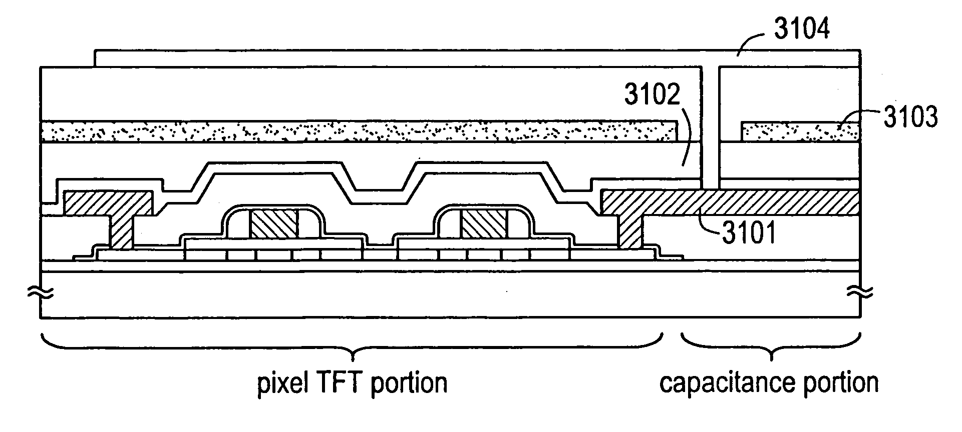
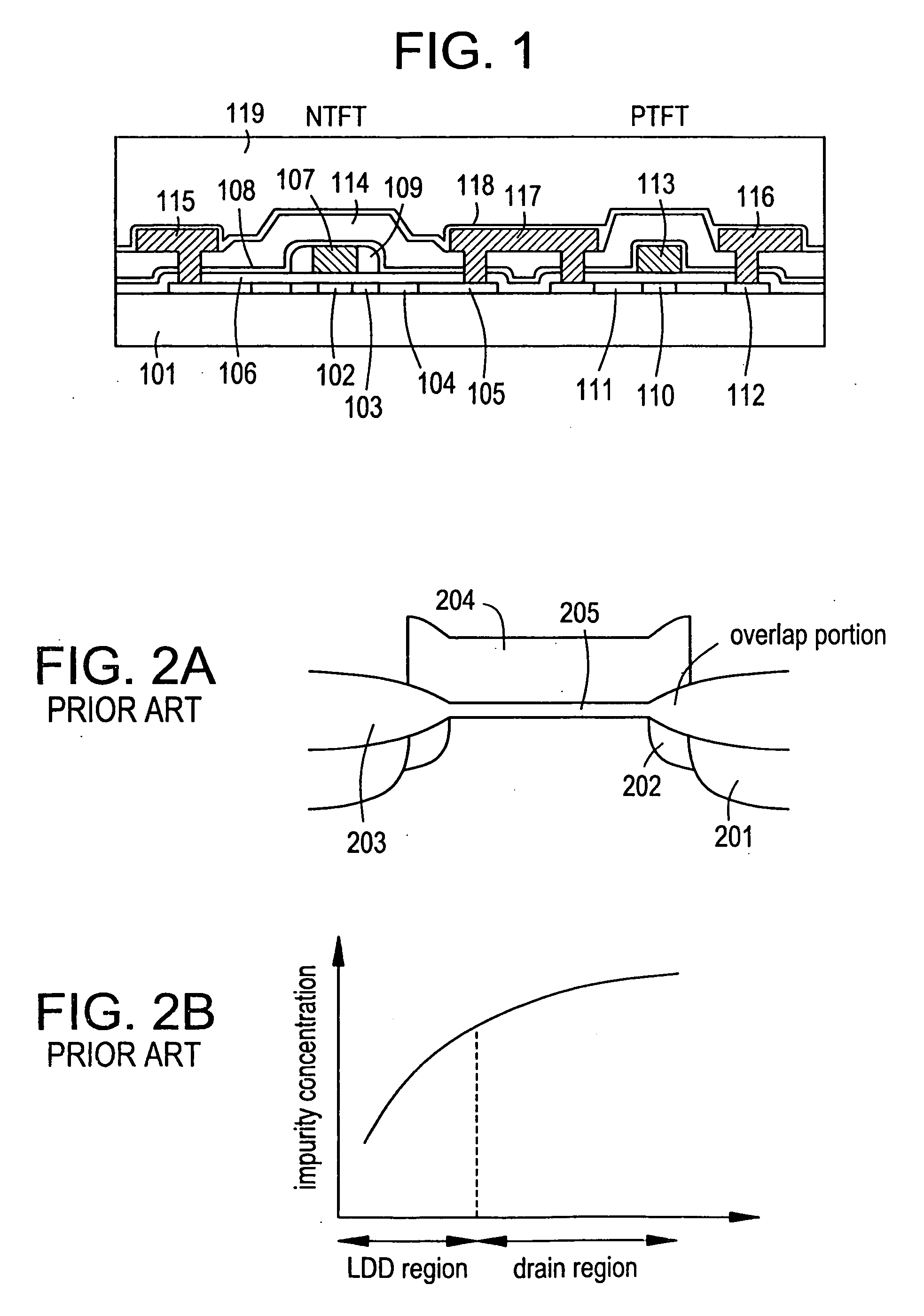
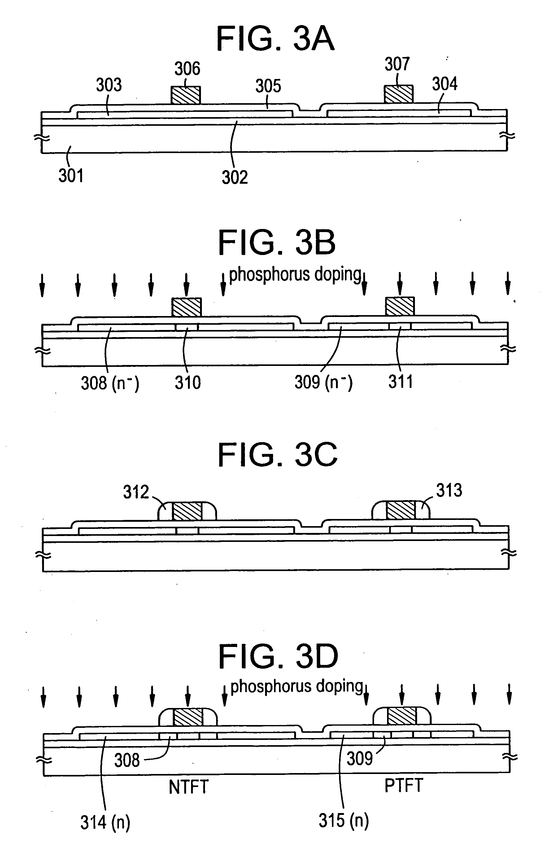
[0179] In this example, a method of manufacturing the CMOS circuit shown in FIG. 1 is to be explained with reference to FIGS. 3A to 3D and FIGS. 4A to 4D.

[0180] At first, an underlying film comprising a silicon oxide film 302 is formed to 200 nm thickness on a glass substrate 301. The underlying film may be a laminated film comprising a silicon nitride film and a silicon oxide film, or consisting of only a silicon nitride film. A plasma CVD method, a thermal CVD method or a sputtering method may be used for the method of forming the film. It is effective to add boron to the silicon nitride film for improving the heat dissipating effect.

[0181] Then, an amorphous silicon film of 50 nm thickness is formed on the silicon oxide film 302 by a plasma CVD method, a heat CVD method or a sputtering method. Then, the amorphous silicon film is crystallized by using the technique described in Japanese Patent Laid-Open No. 7-130652 (1995) to form a semiconductor film containing crystals. The Ja...

example 2

[0220] In Example 1, undoped-Si (intrinsic silicon layer or undoped silicon layer) to which impurities are not added intentionally is used for the side wall, but a phosphorus doped silicon layer (n+ Si layer) in which phosphorus is added upon forming the film or a boron-doped silicon layer (p+ Si layer) is used. Of course, it may be an amorphous, crystalline or microcrystalline material.

[0221] By using phosphorus-added silicon layer or boron-added silicon layer, the resistance in the side wall portion is entirely lowered and a possibility for the fluctuation of characteristics caused by scattering of the profile for the concentration of phosphorus considered for the step in FIG. 3D could be eliminated.

example 3

[0222] In Example 1, undoped-Si in which impurities are not added intentionally is used as the side wall, but a silicon layer containing one of carbon (C), nitrogen (N) or oxygen (O) is used to increase the resistance value of the side wall in this example. Of course, the silicon layer may be formed any of amorphous, crystalline or micro-crystalline material. Further, as the impurity to be used, oxygen is most favorable.

[0223] That is, when a silicon layer as a side wall is formed, carbon, nitrogen or oxygen could be added at 1 to 50 atomic % (typically 10 to 30 atomic %). In this example, 20 atomic % of oxygen is added.

[0224] Since the resistance value due to the side wall is increased with the constitution of this example, it is possible to obtain a constitution in which the effect of the capacitance with the side wall as a dielectric is predominant in applying a gate voltage. That is, an effective gate voltage could be applied also to the side wall portion upon high frequency d...


PUM


Abstract

The active layer of an n-channel TFT is formed with a channel forming region, a first impurity region, a second impurity region and a third impurity region. In this case, the concentration of the impurities in each of the impurity regions is made higher as the region is remote from the channel forming region. Further, the first impurity region is disposed so as to overlap a side wall, and the side wall is caused to function as an electrode to thereby attain a substantial gate overlap structure. By adopting the structure, a semiconductor device of high reliability can be manufactured.

Description

BACKGROUND OF THE INVENTION [0001] 1. Field of the Invention [0002] The present invention concerns a semiconductor device having a circuit constituted with thin film transistors (hereinafter referred to as a TFT). It relates to a constitution of an electro-optic device typically represented by a liquid crystal display panel, and an electronic equipment having such an electro-optic device mounted as a part thereon. The semiconductor device used in the present specification generally means all devices that can operate by utilizing semiconductor characteristics, and electro-optical devices, semiconductor circuits and electronic equipments are also included in the semiconductor device. [0003] 2. Description of the Related Art [0004] In recent years, an active matrix type liquid crystal display device having circuits constituted with TFTs utilizing polysilicon films has been noted. In the device, electric fields applied to liquid crystals are controlled in a matrix form by a plurality of...

Claims


Application Information

Patent Timeline
Patent Type & Authority Applications(United States)
IPC IPC(8): H01L29/76H01L29/94
CPCH01L29/78621H01L27/1277H01L2029/7863H01L2924/0002H01L2924/00
Inventor YAMAZAKI, SHUNPEIOHTANI, HISASHIHAMATANI, TOSHIJI
Owner SEMICON ENERGY LAB CO LTD
Why Eureka
Try Eureka