Semiconductor die package and method for making the same

a technology of semiconductor devices and dies, applied in the field of semiconductor die packages, can solve the problems of many of the above-described packages, and achieve the effect of improving the quality of the produ

Active Publication Date: 2007-01-04
SEMICON COMPONENTS IND LLC
View PDF85 Cites 177 Cited by
  • Summary
  • Abstract
  • Description
  • Claims
  • Application Information

AI Technical Summary

Benefits of technology

[0016] Another embodiment of the invention is directed to a method comprising: obtaining a substrate comprising a conductive die attach surface; attaching a high side transistor including a high side transistor input to the substrate, wherein the high side transistor input is coupled to the conductive die attach surface; and attaching a low side transistor including a low side transistor output to the substrate, wherein the low side transistor input is coupled to the conductive die attach surface.
[0017] Another embodiment of the invention is directed to a semiconductor device package comprising: a substrate comprising a conductive die attach surface; a high side transistor including a high side transistor input, wherein the high side transistor input is coupled to the conductive die attach surface; and a low side transistor including a low side transistor output, wherein the low side transistor input is coupled to the conductive die attach surface.

Problems solved by technology

For example, many of the above-described packages are difficult and / or expensive to make.

Method used


Image

  • Semiconductor die package and method for making the same
  • Semiconductor die package and method for making the same
  • Semiconductor die package and method for making the same

Examples


Embodiment Construction

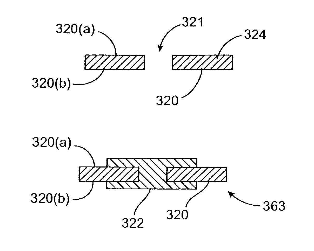
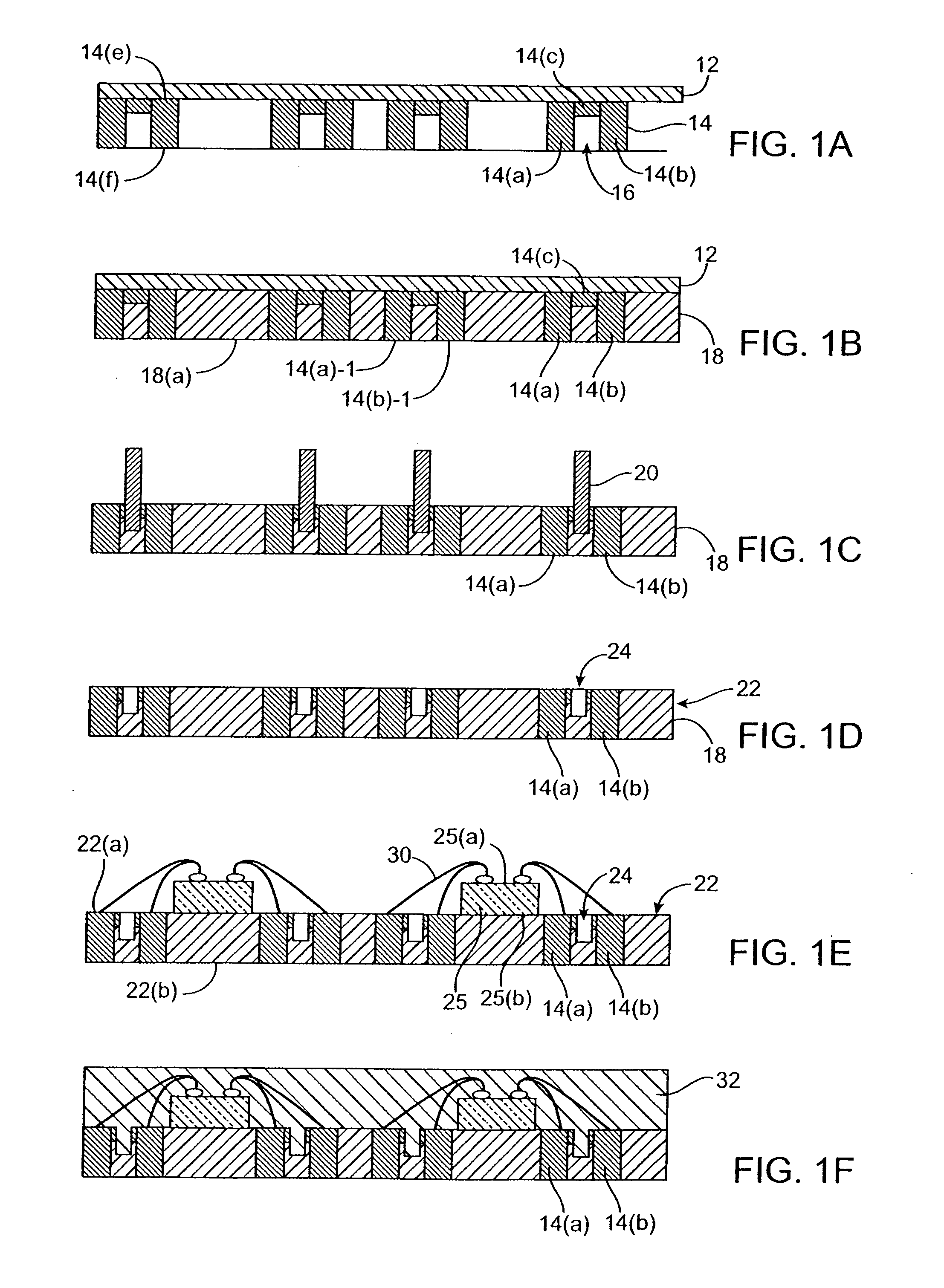
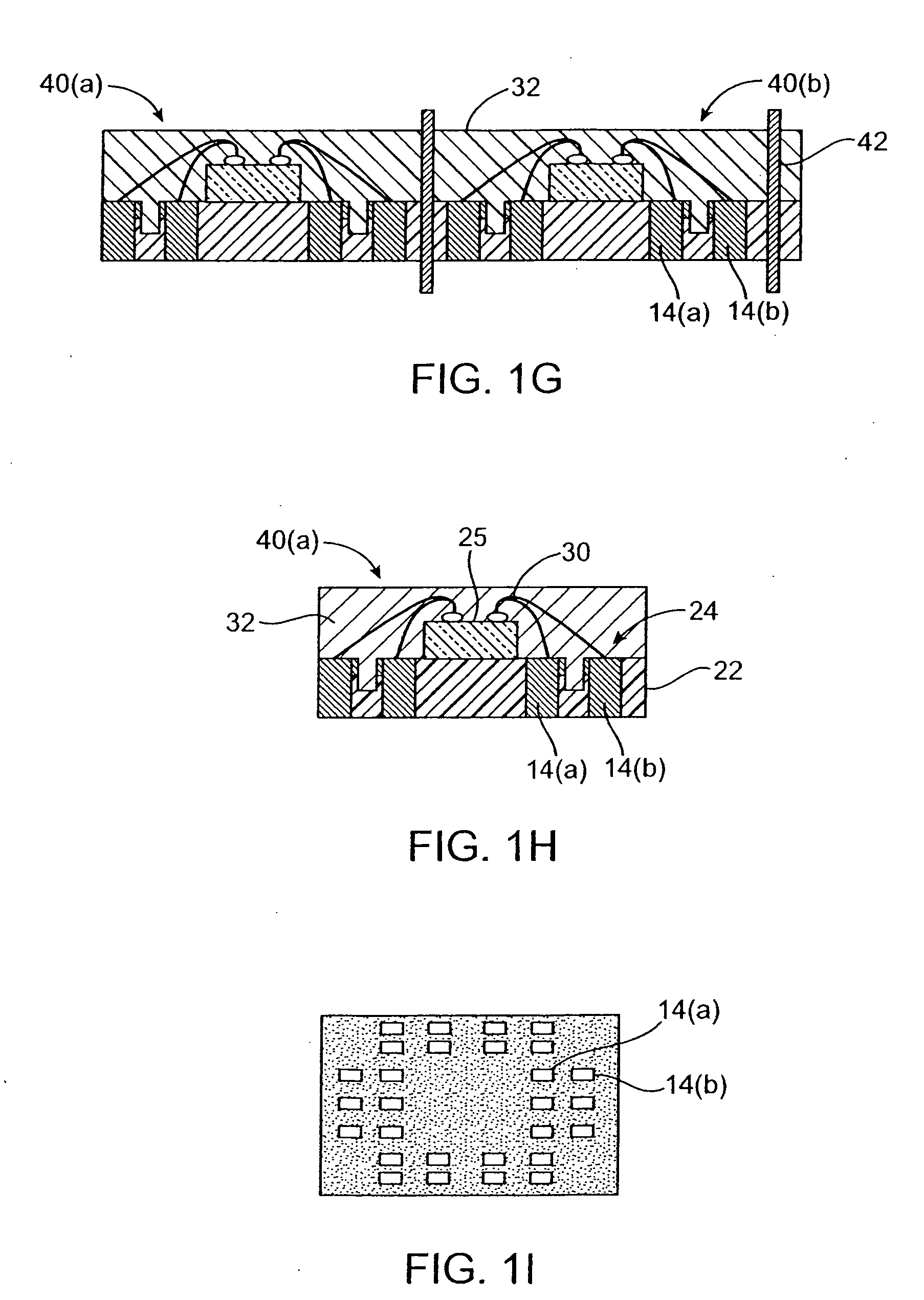
[0088] Embodiments of the invention are directed to semiconductor die packages and methods for making semiconductor die packages. A semiconductor die package according to an embodiment of the invention includes a substrate, and a semiconductor die mounted on the substrate. The semiconductor die may at attached to the substrate using an adhesive or any other suitable attachment material. In the semiconductor die package, the bottom surface and / or the top surface of the semiconductor die may be electrically coupled to conductive regions of the substrate. An encapsulating material may encapsulate the semiconductor die. As will be explained in further detail below, the substrates according to embodiments of the invention can have different configurations in different embodiments.

[0089] The substrate may have any suitable configuration. However, in preferred embodiments of the invention, the substrate includes a leadframe structure and a molding material. Typically, at least one surface...


PUM

PropertyMeasurementUnit
thicknessaaaaaaaaaa
thicknessaaaaaaaaaa
thicknessaaaaaaaaaa

Abstract

Semiconductor die packages are disclosed. An exemplary semiconductor die package includes a premolded substrate. The premolded substrate can have a semiconductor die attached to it, and an encapsulating material may be disposed over the semiconductor die.

Description

CROSS-REFERENCES TO RELATED APPLICATIONS [0001] This patent application is a non-provisional of and claims the benefit of the following U.S. Provisional Applications: 60 / 701,781, filed on Jul. 22, 2005; 60 / 696,320, filed on Jun. 30, 2005; 60 / 696,027, filed on Jun. 30, 2005; 60 / 696,350, filed on Jun. 30, 2005; 60 / 702,076, filed on Jul. 22, 2005; 60 / 696,305, filed on Jun. 30, 2005, and 60 / 753,040, filed on Dec. 21, 2005. These U.S. Provisional Applications are herein incorporated by reference in their entirety for all purposes.BACKGROUND OF THE INVENTION [0002] Various semiconductor die packages are known. [0003] While such packages are useful, they could be improved. For example, many of the above-described packages are difficult and / or expensive to make. [0004] Accordingly, it would be desirable to provide for improved semiconductor die packages, methods for making semiconductor die packages, components of such die packages, and electrical assemblies using such semiconductor die pac...

Claims


Application Information

Patent Timeline
Patent Type & Authority Applications(United States)
IPC IPC(8): H01L21/00
CPCH01L2924/01067H01L2924/014H01L24/29H01L2924/0132H01L2924/1815H01L2224/29111H01L2224/291H01L2924/15747H01L2224/293H01L2224/2919H01L2224/2929H01L2924/00013H01L2224/29299H01L2224/49113H01L24/83H01L2924/1306H01L2924/07802Y10T29/49121H01L2924/1305H01L2924/14H01L2924/19043H01L2924/30107H01L21/561H01L23/3121H01L23/4951H01L23/49558H01L23/49562H01L23/49575H01L23/49861H01L24/32H01L24/39H01L24/45H01L24/49H01L24/97H01L25/0655H01L2223/54406H01L2223/54486H01L2224/16H01L2224/32057H01L2224/45124H01L2224/45139H01L2224/45144H01L2224/45147H01L2224/45565H01L2224/456H01L2224/45644H01L2224/45669H01L2224/48091H01L2224/48137H01L2224/48227H01L2224/48237H01L2224/48247H01L2224/48257H01L2224/48465H01L2224/4943H01L2224/73265H01L2224/83192H01L2224/83385H01L2224/85013H01L2224/97H01L2924/01004H01L2924/01005H01L2924/01013H01L2924/01015H01L2924/01027H01L2924/01028H01L2924/01029H01L2924/01033H01L2924/01046H01L2924/01047H01L2924/0105H01L2924/01074H01L2924/01078H01L2924/01079H01L2924/01082H01L2924/13091H01L24/48H01L2224/32225H01L2224/73204H01L2924/01006H01L2924/01019H01L2924/01023H01L2924/01024H01L2924/00014H01L2224/85H01L2924/00H01L2924/00012H01L2224/13111H01L2924/0665H01L2224/29099H01L2224/29199H01L2224/45015H01L2924/181H01L2224/45169H01L2924/12042H01L2224/40245H01L24/40H01L24/73H01L2224/83801H01L2224/8385H01L2224/16245H01L2224/73221H01L2924/207H01L23/28
Inventor JEON, OSEOBCHOI, YOONHWAGOOI, BOON HUANESTACIO, MARIA CRISTINA B.CHONG, DAVIDKENG, TAN TEIKNAM, SHIBAEKJOSHI, RAJEEVWU, CHUNG-LINIYER, VENKATLIM, LAY YEAPLEE, BYOUNG-OK
Owner SEMICON COMPONENTS IND LLC
Why Eureka
Try Eureka