Integrated semiconductor circuits on photo-active Germanium substrates

a germanium substrate and integrated semiconductor technology, applied in the field of semiconductor devices, can solve the problems of high use and manufacturing costs, the substrate cannot be used to the device formation in the substrate itself, and the technology is limited to photovoltaic applications, and achieve the effect of less expensiv

Inactive Publication Date: 2005-05-26
THE BOEING CO
View PDF8 Cites 196 Cited by
  • Summary
  • Abstract
  • Description
  • Claims
  • Application Information

AI Technical Summary

Benefits of technology

[0011] It is thus an object of the present invention to create a less expensive and functionally different optoele

Problems solved by technology

The disadvantage of these intrinsic substrates is their high cost of use and manufacture.
These substrates cannot be used to the device formation in the substrate itself.
To date, it is believed that this technology has been limited to photovoltaic applications.
One problem with currently available technology is the cost of using a conventional substrate

Method used


Image

  • Integrated semiconductor circuits on photo-active Germanium substrates
  • Integrated semiconductor circuits on photo-active Germanium substrates
  • Integrated semiconductor circuits on photo-active Germanium substrates

Examples


Embodiment Construction

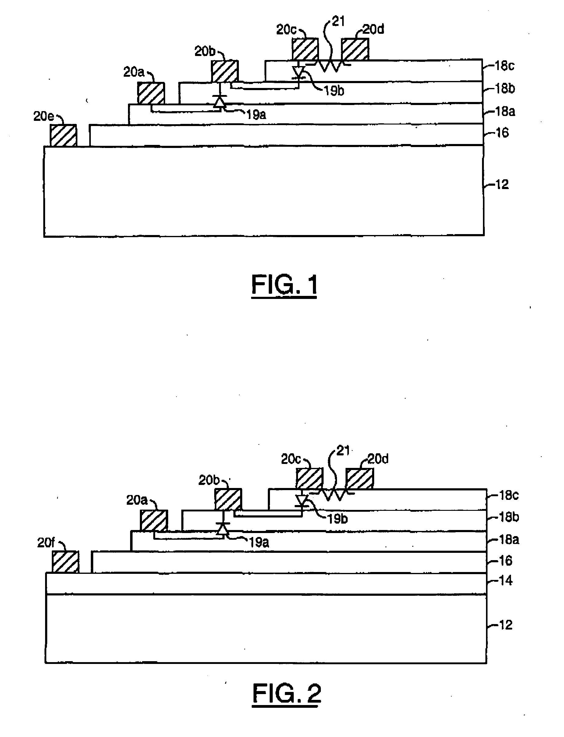
[0021]FIGS. 1 and 2 show schematic representations of forming a semiconductor device 10 that is used to form an optoelectronic integrated circuit that is the heart of the present invention.

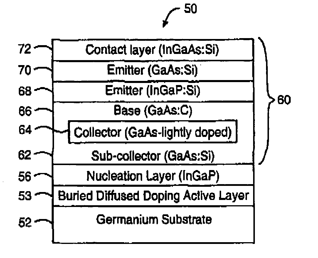
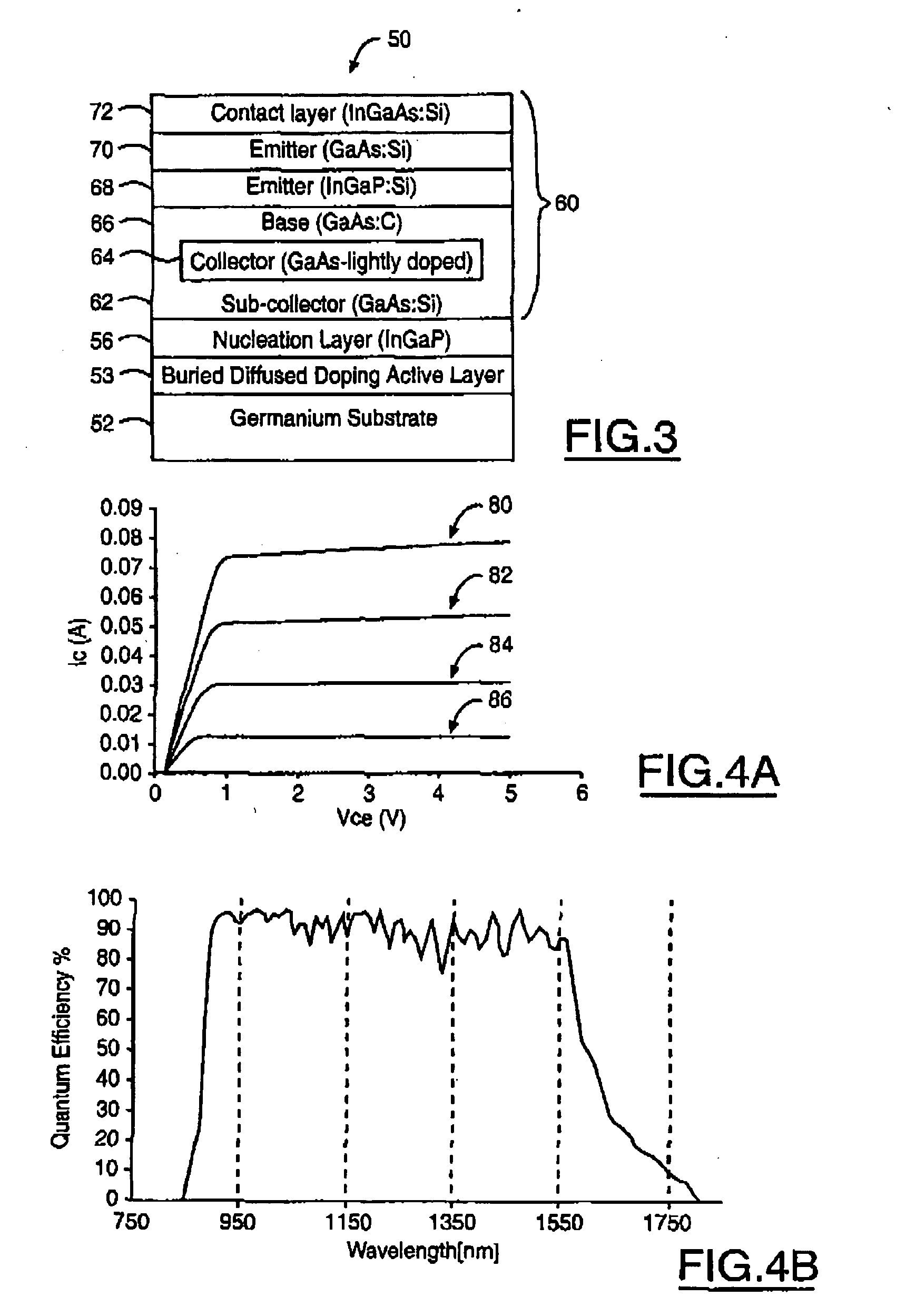
[0022] Referring now to FIG. 1, a schematic representation of a semiconductor device 10, according to one preferred embodiment is depicted as consisting of a germanium substrate 12, a nucleation layer 16, a series of III-V epitaxial layers 18, and a plurality of electrical contacts 20. In an alternative preferred embodiment, as shown in FIG. 2, a buried germanium diffused-doping active layer 14, is formed on a top portion of the germanium substrate 12 adjacent to the nucleation layer 16.

[0023] Preferably, the III-V semiconductor compounds used in the epitaxial layers 18 of the optoelectronic circuits are (Al, In, Ga) arsenide compounds and / or (Al, In, Ga) phosphide compounds that are grown on, germanium substrates 12.

[0024] To form the device 10, the germanium substrate 12 is loaded in a metal-...


PUM


Abstract

A semiconductor device having at least one layer of a group III-V semiconductor material epitaxially deposited on a group III-V nucleation layer adjacent to a germanium substrate. By introducing electrical contacts on one or more layers of the semiconductor device, various optoelectronic and microelectronic circuits may be formed on the semiconductor device having similar quality to conventional group III-V substrates at a substantial cost savings. Alternatively, an active germanium device layer having electrical contacts may be introduced to a portion of the germanium substrate to form an optoelectronic integrated circuit or a dual optoelectronic and microelectronic device on a germanium substrate depending on whether the electrical contacts are coupled with electrical contacts on the germanium substrate and epitaxial layers, thereby increase the functionality of the semiconductor devices.

Description

RELATED APPLICATION [0001] The present application is a continuation-in-part (CIP) application of U.S. patent application Ser. No. 09 / 850,773 filed on May 8, 2001 entitled “Semiconductor Circuits And Devices On Germanium Substrates” (Attorney Docket Number OC 0128 PA), which is incorporated by reference herein.TECHNICAL FIELD [0002] The present invention generally relates to semiconductor devices and, more particularly, semiconductor circuits and devices on germanium substrates with a photoactive junction. BACKGROUND ART [0003] It is known to use germanium as a substrate material for epitaxial growth of III-V materials. Germanium is a substrate of choice the space solar cell industry for GaAs and GaInP / GaAs substrates. In this application, germanium substrate is used either with an active semiconductor junction inside of the Germanium substrate or without an active junction in Germanium. [0004] Devices that use these III-V materials are typically photonic devices such as solar cells...

Claims


Application Information

Patent Timeline
IPC IPC(8): H01L31/0328H01L31/18
CPCH01L21/02381H01L21/02461Y02E10/544H01L21/02546H01L31/1852H01L21/02543
Inventor BOUTROS, KARIM S.KARAM, NASSER H.KRUT, DIMITRIHADDAD, MORAN
Owner THE BOEING CO
Why Eureka
Try Eureka