

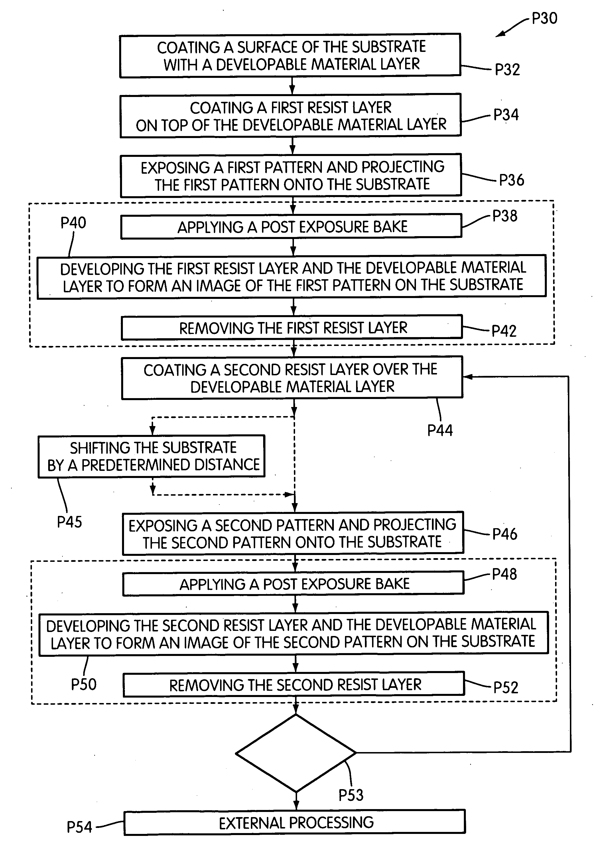
Reduced pitch multiple exposure process
a multiple exposure and process technology, applied in photographic processes, printers, electrostatic spraying apparatus, etc., can solve the problems of reduced cd, limited process latitude, and difficult fabrication of contact holes, etc., and achieve the effect of enhancing image resolution
- Summary
- Abstract
- Description
- Claims
- Application Information
AI Technical Summary
Benefits of technology
Problems solved by technology
Method used
Image

Examples
Embodiment Construction
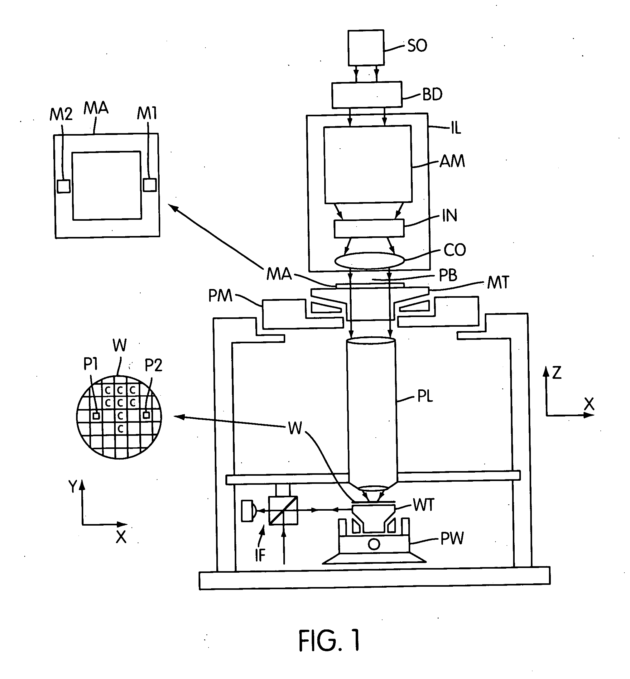
[0037]FIG. 1 schematically depicts a lithographic apparatus according to a particular embodiment of the invention. The apparatus includes:
[0038] an illumination system (illuminator) IL adapted to condition a beam PB of radiation (e.g., UV radiation);
[0039] a support structure (e.g., a mask table) MT configured to hold a patterning device (e.g., a mask) MA and connected to first positioning device PM configured to accurately position the patterning device with respect to item PL;
[0040] a substrate table (e.g., a wafer table) WT configured to hold a substrate (e.g., a resist-coated wafer) W and connected to second positioning device PW configured to accurately position the substrate with respect to item PL; and
[0041] a projection system (e.g., a refractive projection lens) PL adapted to image a pattern imparted to the beam PB by the patterning device MA onto a target portion C (e.g., comprising one or more dies) of the substrate W.
[0042] As here depicted, the apparatus is of a tr...
PUM
 Abstract
Description
Claims
Application Information