Structure and method for producing multiple size interconnections

a technology of interconnection and structure, applied in the direction of printed circuit, sustainable manufacturing/processing, final product manufacturing, etc., can solve the problem that the substrate may not be large enough to accommodate the large number of connections

Active Publication Date: 2007-01-11
AURIGA INNOVATIONS INC
View PDF9 Cites 39 Cited by
  • Summary
  • Abstract
  • Description
  • Claims
  • Application Information

AI Technical Summary

Problems solved by technology

Joining substrates together in electrical applications typically requires a large number of connections be

Method used


Image

  • Structure and method for producing multiple size interconnections
  • Structure and method for producing multiple size interconnections
  • Structure and method for producing multiple size interconnections

Examples


Embodiment Construction

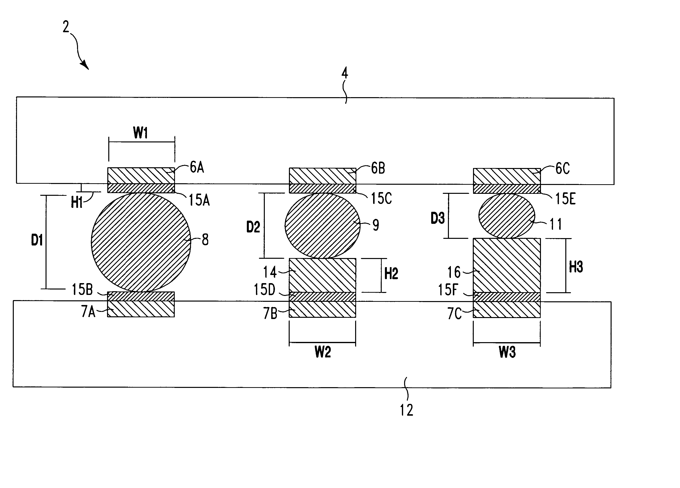
[0010]FIG. 1 illustrates a cross-sectional view of an electrical structure 2 having a substrate 4 electrically and mechanically connected to a substrate 12 using a plurality of different sized controlled collapse chip connection (C4) solder balls 8, 9, and 11, in accordance with embodiments of the present invention. Alternatively, the C4 solder balls 8, 9, and 11 may comprise any type of electrical interconnection for electrically and mechanically connecting a substrate 4 to a substrate 12. Note that the C4 solder balls 8, 9, and 11 are shown for illustration purposes and that an unlimited number of C4 solder balls similar to the C4 solder balls 8, 9, and 11 (or any type of interconnections) may be used to electrically and mechanically connect to the substrate 4 to the substrate 12. The C4 solder balls 8, 9, and 11 each comprise a different size (i.e., a different diameter). The different sized C4 solder balls 8, 9, and 11 are used to carry different types of signals between the sub...


PUM


Abstract

An electrical structure and method comprising a first substrate electrically and mechanically connected to a second substrate. The first substrate comprises a first electrically conductive pad and a second electrically conductive pad. The second substrate comprises a third electrically conductive pad, a fourth electrically conductive pad, and a first electrically conductive member. The fourth electrically conductive pad comprises a height that is different than a height of the first electrically conductive member. The electrically conductive member is electrically and mechanically connected to the fourth electrically conductive pad. A first solder ball connects the first electrically conductive pad to the third electrically conductive pad. The first solder ball comprises a first diameter. A second solder ball connects the second electrically conductive pad to the first electrically conductive member. The second solder ball comprises a second diameter. The first diameter is greater than said second diameter.

Description

TECHNICAL FIELD [0001] The present invention relates to an electrical structure for producing multiple size interconnections between substrates. RELATED ART [0002] Joining substrates together in electrical applications typically requires a large number of connections between the substrates. The substrates may not be large enough to accommodate the large number of connections. Therefore there exists a need to accommodate the large number of connections necessary to join substrates together in electrical applications. SUMMARY OF THE INVENTION [0003] The present invention provides an electrical structure, comprising: a first substrate comprising a first electrically conductive pad and a second electrically conductive pad; a second substrate comprising a third electrically conductive pad, a fourth electrically conductive pad, and a first electrically conductive member, wherein said electrically conductive member is electrically and mechanically connected to said fourth electrically cond...

Claims


Application Information

Patent Timeline
IPC IPC(8): H01L23/48
CPCH01L23/13H01L2224/06102H01L23/49816H01L23/49838H01L24/11H01L24/12H01L24/17H01L24/73H01L24/81H01L2224/0401H01L2224/0603H01L2224/13099H01L2224/1403H01L2224/49109H01L2224/81801H01L2924/01029H01L2924/01047H01L2924/01082H01L2924/01322H05K3/3436H05K2201/094H05K2201/09736H05K2201/09845H01L24/49H01L2924/01006H01L2924/0105H01L2924/014H01L2924/00013H01L23/49811H01L2224/13111H01L2224/131H01L2224/29099H01L2924/00014Y02P70/50H01L2224/45099H01L2224/45015H01L2924/207
Inventor CLEVENGER, LAWRENCEFAROOQ, MUKTA G.HSU, LOUIS L.LANDERS, WILLIAM F.ZUPANSKI-NIELSEN, DONNA S.RADENS, CARL J.YANG, CHIH-CHAO
Owner AURIGA INNOVATIONS INC
Why Eureka
Try Eureka