Integrated compact MEMS device with deep trench contacts

a compact, mems technology, applied in the direction of microstructural devices, instruments, forming microstructure systems, etc., can solve the problems of complex packaging process, wafer level flip chip technology cannot be used in fabricating mems devices, and achieve high aspect ratio deep trench contacts

Inactive Publication Date: 2013-07-04
WINDTOP TECH CORP
View PDF6 Cites 108 Cited by
  • Summary
  • Abstract
  • Description
  • Claims
  • Application Information

AI Technical Summary

Benefits of technology

[0005]The primary object of the present invention is to provide a novel structure of single-chip compact MEMS motion sensor, wherein MEMS is made with CMOS wafer as a foundation to form a single chip compact MEMS device compatible with flip chip package capability. The present invention utilizes CMOS trench polysilicon interconnects for MEMS signal and anchors. The advantage to use polysilicon deep trench interconnect is that polysilicon deep trench is compatibility with CMOS process in term of material characteristics and also conformal during film deposition so that high aspect ratio deep trench contacts and thus interconnects can be realized.

Problems solved by technology

The drawbacks are that package processes are often complicated because wafer probing is needed on both MEMS and ASIC dies separately.
Since the signals from MEMS dies are very small, the wafer probing on it is quite a challenge.
By using the conventional methods to form MEMS devices, wafer level flip chip technology cannot be used in fabricating MEMS devices.
However, the drawbacks of these methods are that Flip Chip bumping process cannot be performed and thus neither wafer-level package (WLP) nor chip scale package (CSP) are possible.

Method used


Image

  • Integrated compact MEMS device with deep trench contacts
  • Integrated compact MEMS device with deep trench contacts
  • Integrated compact MEMS device with deep trench contacts

Examples


Embodiment Construction

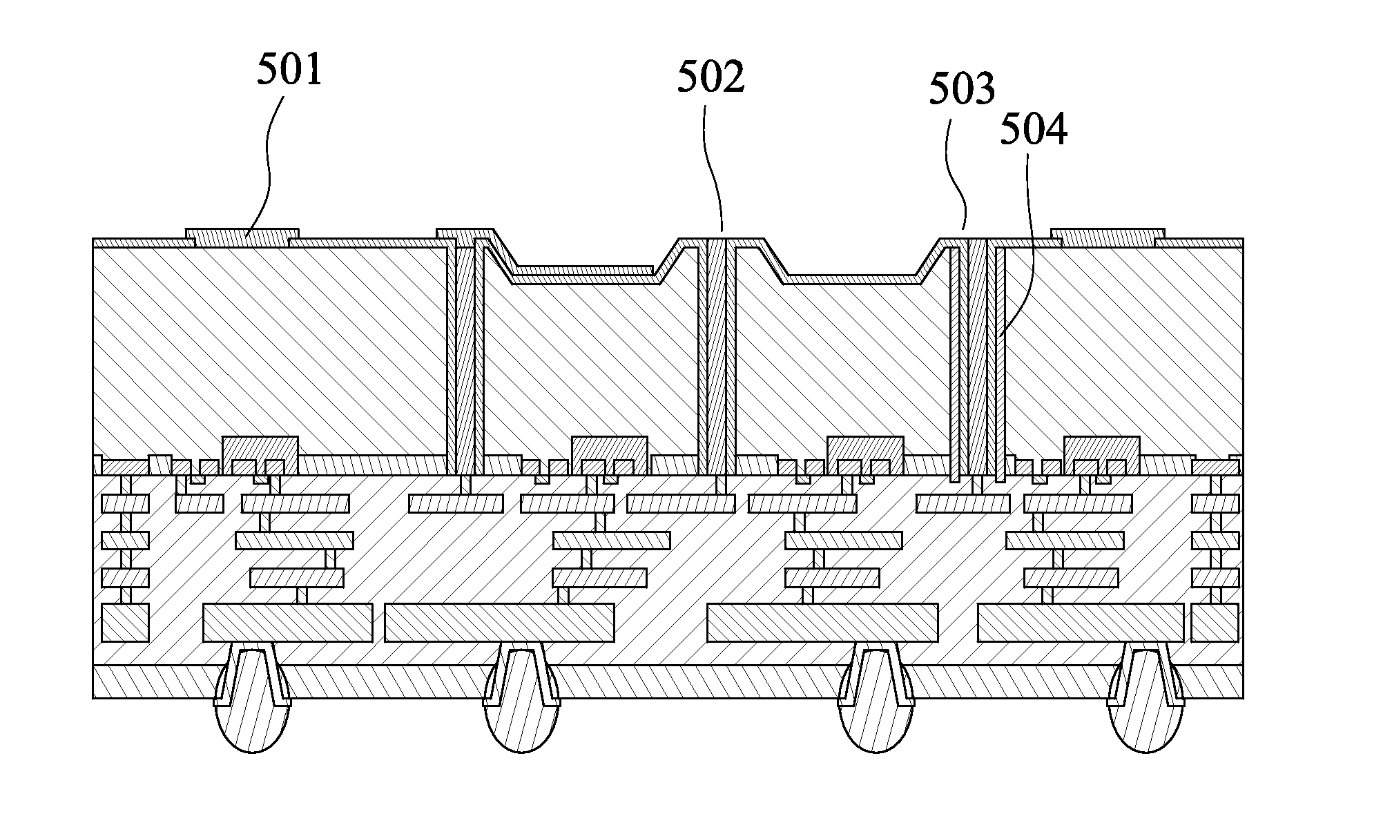
[0021]FIG. 2 shows a schematic view of an exemplary embodiment of a structure of an integrated compact MEMS device made with the flip chip technology according to the present invention. However, if the CMOS ASIC circuit is made with bond pads for wire bonding, the resulting device based on the present invention will yield an integrated MEMS device for a lead frame base wire bonding package. As shown in FIG. 2, the compact MEMS device of a motion sensor includes a CMOS substrate layer 201 made of Si silicon, with a plurality of anchor posts penetrating CMOS substrate layer having an isolation oxide layer 202 on the outside surrounding a conductive layer 203. On one side of CMOS substrate layer 201, the structure of the present invention further includes a field oxide (FOX) layer 204, a first set of implant doped silicon areas 205, a second set of implant doped silicon areas 206, a first polysilicon layer 207, an oxide layer 208 embedded with a plurality of metal layers interleaved wi...


PUM


Abstract

A compact MEMS motion sensor device is provided, including a CMOS substrate layer, with plural anchor posts having an isolation oxide layer surrounding a conductive layer. On one side of CMOS substrate layer, the device further includes a field oxide (FOX) layer, a first set and a second set of implant doped silicon areas, a first polysilicon layer, an oxide layer embedded with plural metal layers interleaved with via hole layers, a Nitride deposition layer, an under bump metal (UBM) layer and a plurality of solder spheres. On the other side of CMOS substrate layer, the present invention further includes a backside interconnect isolation oxide layer, a first MEMS bonding layer, a first metal compound layer, a second MEMS bonding layer, a MEMS layer, a first MEMS eutectic bonding layer, a second metal compound layer, a second MEMS eutectic bonding layer, and a MEMS cap layer.

Description

FIELD OF THE INVENTION[0001]The present invention generally relates to an integrated compact MEMS device with deep trench contacts, and more specifically to an integrated compact MEMS device with deep trench polysilicon contacts to connect CMOS ASIC circuit and MEMS module, applicable to both wafer-level flip chip package and wire bonding technologies.BACKGROUND OF THE INVENTION[0002]Most of the conventional MEMS devices or motion sensors have been composed of a MEMS die and an ASIC die, and then a wire bonding package technology is used to bond these two dies together. FIG. 1A shows a schematic view of an exemplary wire bonding package embodiment. As shown in FIG. 1A, a MEMS die 102 and an ASIC die 103 are attached to a lead frame 101. Bond wires 104 are then used to connected MEMS die 102, ASIC die 103 and lead frame 101. A CAP 105 is then attached to MEMS die 102. The drawbacks are that package processes are often complicated because wafer probing is needed on both MEMS and ASIC ...

Claims


Application Information

Patent Timeline
Patent Type & Authority Applications(United States)
IPC IPC(8): H01L29/84
CPCH01L2924/00014H01L24/32H01L2224/29011G01C19/5783G01P1/02H01L2224/48091H01L2224/48137H01L2224/48145H01L2224/29124H01L24/29H01L2924/01322H01L2224/13111H01L2224/131B81C1/00238B81B2201/0235B81B2207/012B81C2203/0792H01L2924/10253H01L2224/05655H01L2224/05647H01L2224/32145H01L2224/73253H01L2224/73265H01L2224/92225H01L2224/94H01L2224/05568H01L2224/05572H01L2224/05624H01L2224/04042H01L2224/0401H01L24/94H01L24/92H01L24/83H01L2924/1461H01L2924/3025H01L24/73H01L24/48H01L2224/83005H01L24/05H01L2224/45099H01L2924/00H01L2924/014H01L2224/83H01L2224/03H01L2224/11H01L2924/01014H01L2224/05552H01L2924/16235H01L2924/00012
Inventor CHEN, KUN-LUNG
Owner WINDTOP TECH CORP
Why Eureka
Try Eureka