Inter-connecting structure for semiconductor device package and method of the same

a technology of interconnection structure and semiconductor device, which is applied in the direction of semiconductor devices, semiconductor/solid-state device details, electrical apparatus, etc., can solve the problems of poor thermal dissipation performance, inability to meet the demand of producing smaller chips with high density elements on the chip, etc., to achieve high reliability and low cost. , the effect of high performan

Inactive Publication Date: 2009-07-02
ADVANCED CHIP ENG TECH
View PDF0 Cites 108 Cited by
  • Summary
  • Abstract
  • Description
  • Claims
  • Application Information

AI Technical Summary

Benefits of technology

[0006]An object of the present invention is to provide a semiconductor device package (chip assembly) that provides a low cost, high performance and high reliability package.

Problems solved by technology

As a semiconductor become more complicated, the traditional package technique, for example lead frame package, flex package, rigid package technique, can't meet the demand of producing smaller chip with high density elements on the chip.
Typical BGA packages include a convoluted signal path, giving rise to high impedance and an inefficient thermal path which results in poor thermal dissipation performance.
Further, the solder is typically a tin-lead alloy and lead-based materials are becoming far less popular due to environmental concerns over disposing of toxic materials and leaching of toxic materials into ground water supplies.
Furthermore, because conventional package technologies have to divide a dice on a wafer into respective dies and then package the die respectively, therefore, these techniques are time consuming for manufacturing process.
Since the chip package technique is highly influenced by the development of integrated circuits, therefore, as the size of electronics has become demanding, so does the package technique.

Method used


Image

  • Inter-connecting structure for semiconductor device package and method of the same
  • Inter-connecting structure for semiconductor device package and method of the same
  • Inter-connecting structure for semiconductor device package and method of the same

Examples


Embodiment Construction

[0021]The invention will now be described in greater detail with preferred embodiments of the invention and illustrations attached. Nevertheless, it should be recognized that the preferred embodiments of the invention is only for illustrating. Besides the preferred embodiment mentioned here, present invention can be practiced in a wide range of other embodiments besides those explicitly described, and the scope of the present invention is expressly not limited expect as specified in the accompanying Claims.

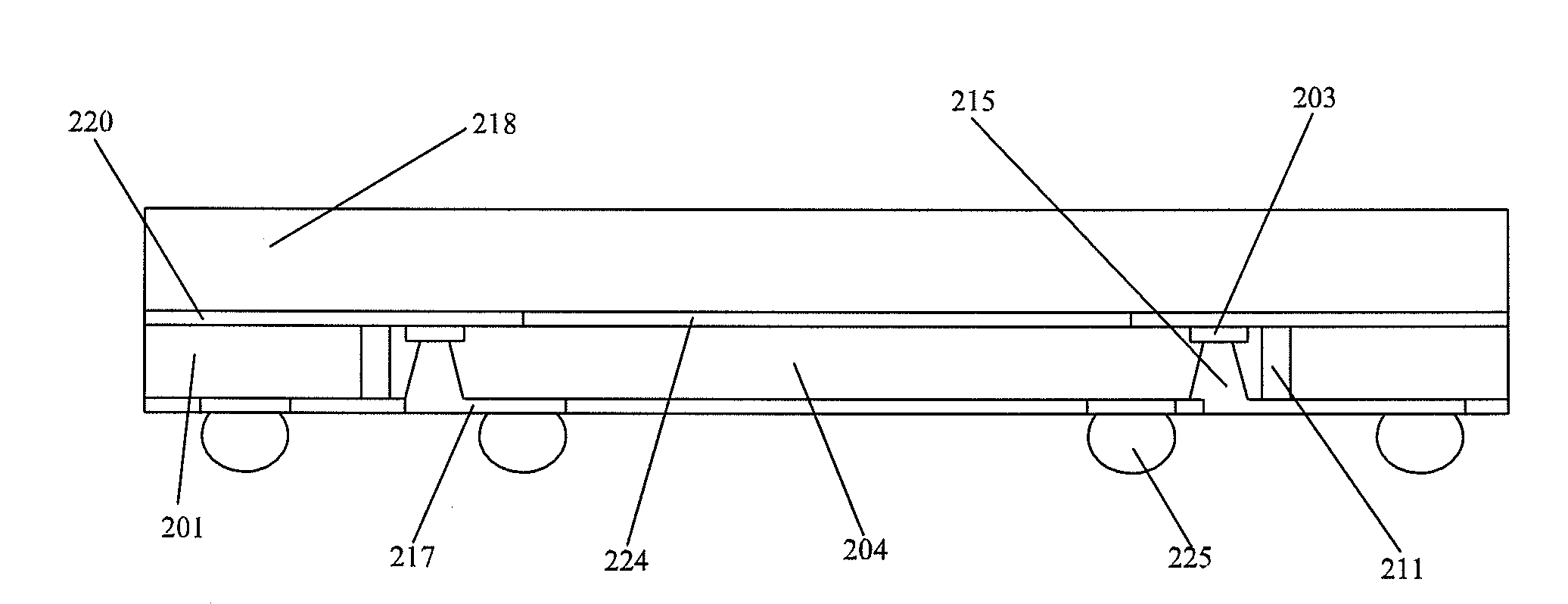
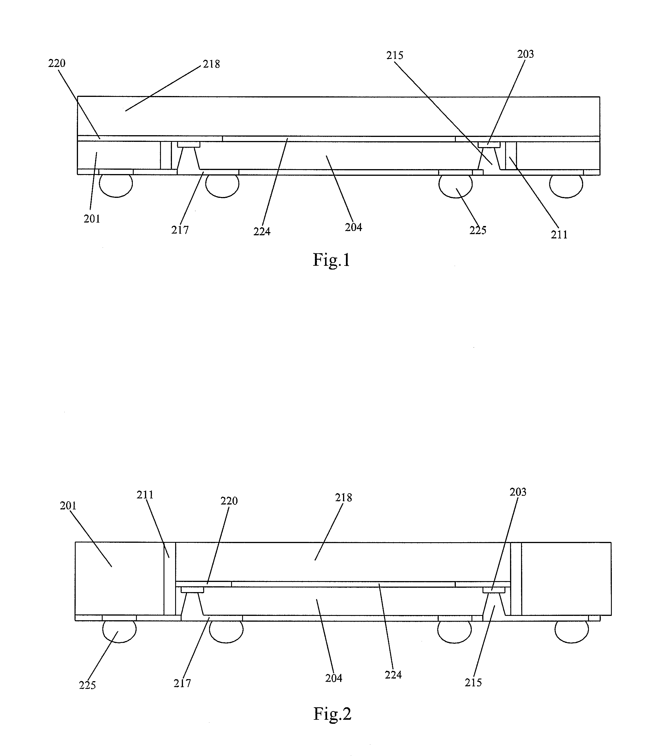
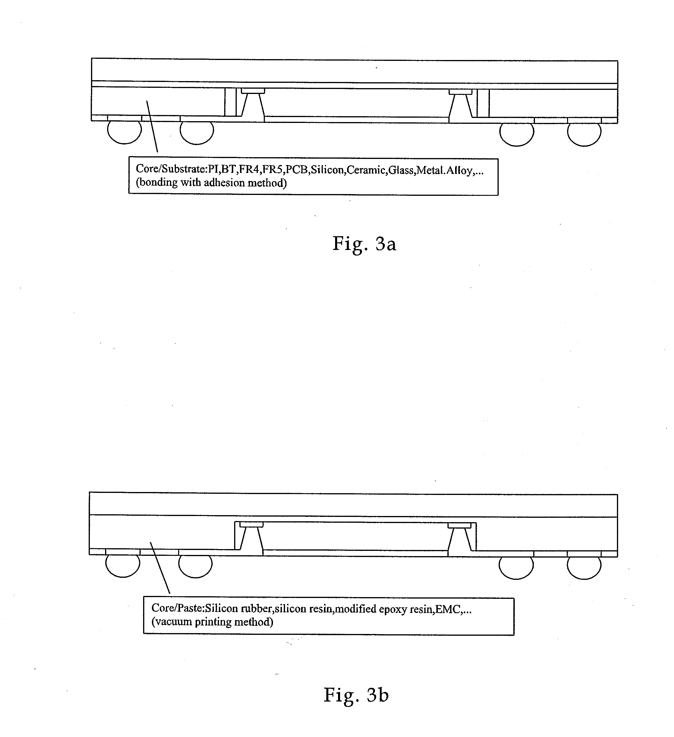
[0022]The present invention discloses a semiconductor device package structure. The present invention provide a semiconductor chip assembly which includes chip, conductive trace and metal inter-connecting as shown in FIG. 1.

[0023]FIG. 1 is cross-sectional view of a substrate (core) 201. The core 201 has a die receiving window 202 for receiving a die 204. The die is CMOS sensor for one embodiment. It could be a single or multi-layer substrate. The chip 204 is adhesion on the surfac...


PUM


Abstract

The interconnecting structure for a semiconductor die includes a die having bonding pads on an active surface; a core attached the side wall (edge) of the die by adhesion material; an isolating base adhered on the active surface of the die by adhesion glue; a through silicon via (TSV) open from the back side of the die to expose the bonding pads; a build up layer coupled between the bonding pads to terminal metal pads by the through silicon via; solder balls melted on terminal pads, wherein the terminal pads located on the core and/or the die.

Description

FIELD OF THE INVENTION [0001]This invention relates to a semiconductor device package, and more particularly to an inter-connecting structure of package.BACKGROUND OF THE INVENTION [0002]The function of chip package includes power distribution, signal distribution, heat dissipation, protection and support. As a semiconductor become more complicated, the traditional package technique, for example lead frame package, flex package, rigid package technique, can't meet the demand of producing smaller chip with high density elements on the chip. In general, array packaging such as Ball Grid Array (BGA) packages provide a high density of interconnects relative to the surface area of the package. Typical BGA packages include a convoluted signal path, giving rise to high impedance and an inefficient thermal path which results in poor thermal dissipation performance. With increasing package density, the spreading of heat generated by the device is increasingly important. In order to meet pack...

Claims


Application Information

Patent Timeline
Patent Type & Authority Applications(United States)
IPC IPC(8): H01L23/498H01L21/60
CPCH01L23/481H01L23/49816H01L2225/1058H01L23/49827H01L23/49833H01L24/24H01L24/29H01L24/82H01L25/0655H01L25/0657H01L25/105H01L27/14618H01L2224/24137H01L2225/06524H01L2225/06541H01L2225/06572H01L2225/06582H01L2924/01013H01L2924/01029H01L2924/01059H01L2924/01078H01L2924/01079H01L2924/01082H01L2924/078H01L2924/09701H01L2924/14H01L2924/15311H01L2924/3011H01L2924/01033H01L2924/01075H01L2225/1035H01L2924/3512H01L2924/00H01L2224/12105H01L2224/73267
Inventor YANG, WEN-KUNCHANG, JUI-HSIENLEE, CHI-CHENTSAI, MON-CHIN
Owner ADVANCED CHIP ENG TECH
Why Eureka
Try Eureka