Semiconductor package with improved ball land structure

a technology of semiconductors and ball land, applied in the direction of printed circuits, sustainable manufacturing/processing, final product manufacturing, etc., can solve the problems of solder ball lands, solder ball cracks or detached from solder ball land, etc., to achieve enhanced connections and improved ball land structures

Active Publication Date: 2006-06-20
SAMSUNG ELECTRONICS CO LTD
View PDF12 Cites 109 Cited by
  • Summary
  • Abstract
  • Description
  • Claims
  • Application Information

AI Technical Summary

Benefits of technology

[0015]It is therefore an object of the present invention to provide semiconductor packages having improved ball land structures, especially, to allow stabilized and enhanced connections between solder balls and a substrate.

Problems solved by technology

In the case of SMD type, during a solder joint reliability test that evaluates a joining strength of the solder ball after the BGA package is mounted on the motherboard, the solder ball is often cracked or detached from the solder ball land.
These issues related to the solder ball lands often arise in another types of packages, using solder ball connections, such as wafer-level packages, flip-chip packages, and so on.

Method used


Image

  • Semiconductor package with improved ball land structure
  • Semiconductor package with improved ball land structure
  • Semiconductor package with improved ball land structure

Examples


first embodiment

[0036

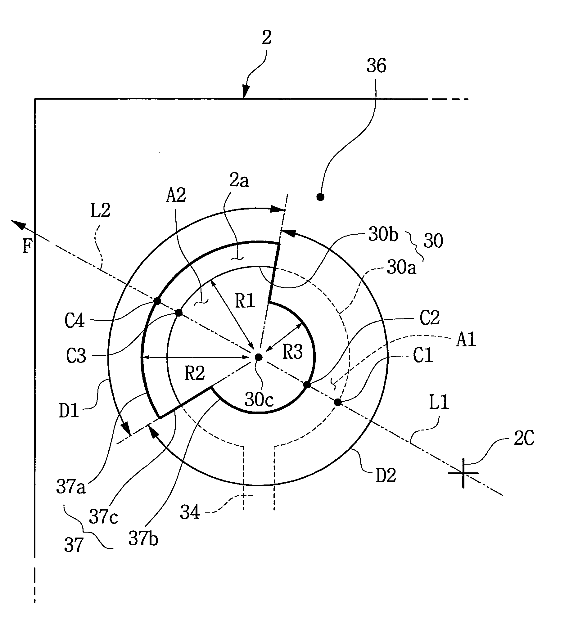
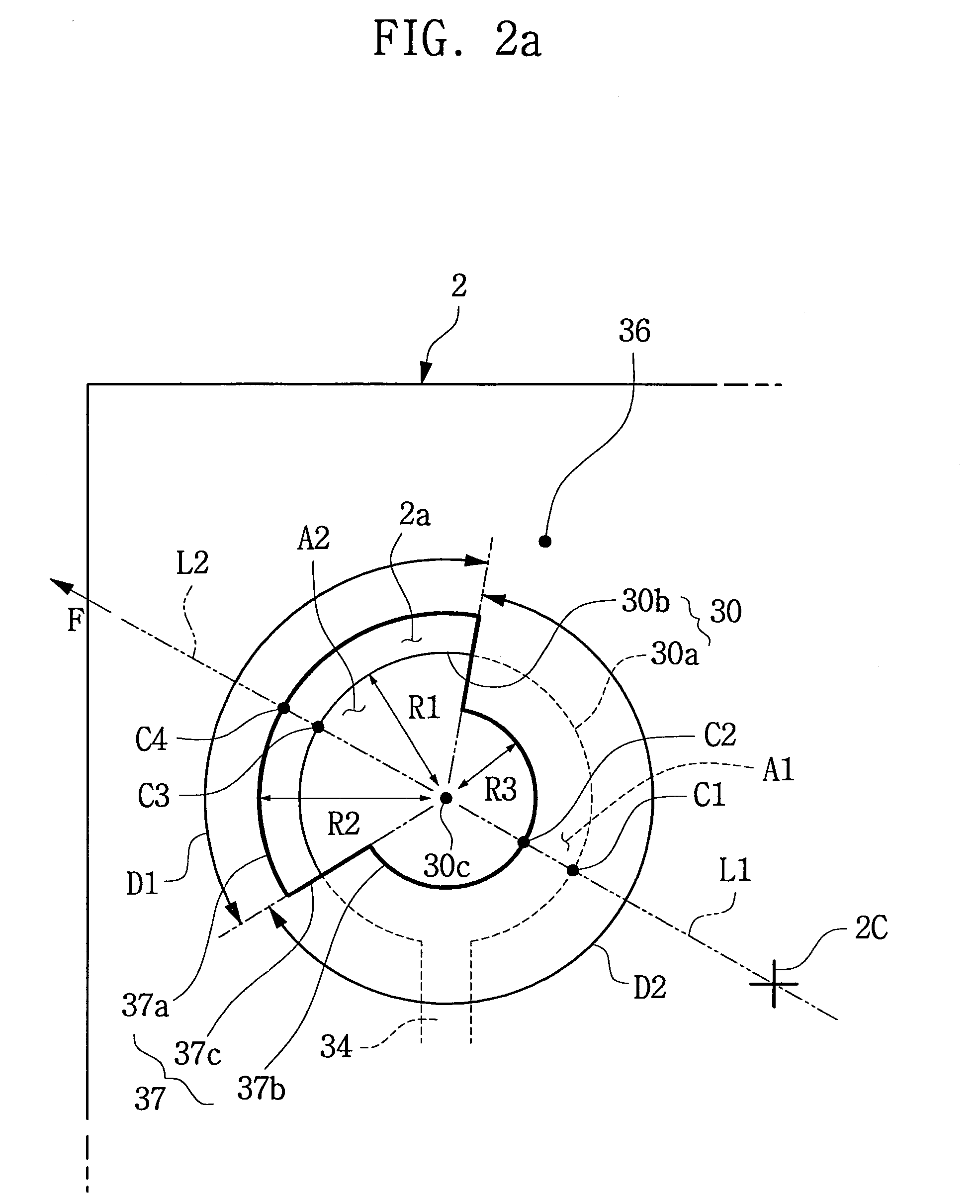
[0037]FIGS. 2A and 2B show, in plan views, a solder ball land of a BGA package in accordance with one embodiment of the present invention. Referring to FIGS. 2A and 2B, a solder ball land 30 is formed on a ball-mounting surface 2 of a substrate used for a BGA package (not shown). A solder mask 36 covers the ball-mounting surface 2, defining an opening area 37.

[0038]A first straight line L1 starts from a land center 30c of the solder ball land 30 and extends toward a central point 2C of the ball-mounting surface 2. The first straight line L1 intersects a land edge 30a of the solder ball land 30 at a first point C1. A distance between the first point C1 and the land center 30c is defined as a first distance W1. Further, the first straight line L1 intersects a second opening edge 37b of the opening area 37 at a second point C2. A distance between the second point C2 and the land center 30c is defined as a second distance W2. As best shown in FIG. 2B, the first distance W1 is longe...

second embodiment

[0044

[0045]FIG. 3 shows, in a plan view, a ball-mounting surface of a BGA package in accordance with another embodiment of the present invention.

[0046]As shown in FIG. 3, the ball-mounting surface 2 of the BGA package is almost covered with the solder mask 36, except a plurality of opening areas 37. Further, a plurality of solder ball lands 30 are formed on the ball-mounting surface 2, and each solder ball land 30 is partially exposed through the respective one opening area 37.

[0047]In each of the solder ball lands 30, the first peripheral portion A1 forming the SMD type structure is disposed to face the central point 2C of the ball-mounting surface 2, whereas the second peripheral portion A2 forming the NSMD type structure is disposed to face the opposite direction to the central point 2C. This composite structure provides more stable and enhanced connection between the solder ball (not shown) and the ball-mounting surface 2, even though the ball-mounting surface 2 is warped due to...

third embodiment

[0048

[0049]FIG. 4 shows, in a plan view, a solder ball land of a BGA package in accordance with still another embodiment of the present invention.

[0050]As shown in FIG. 4, a solder ball land 40 and a wiring pattern 44 electrically connected thereto are formed on the ball-mounting surface 2. Further, the solder mask 36 covers the ball-mounting surface 2, defining an opening area 47. The solder ball land 40 has a first land edge 40a and a second land edge 40b, which are preferably shaped like an arc. The opening area 47 is shaped like a circle having a fourth radius R4. Preferably, a land center 40c coincides with a center of the opening area 47. In the solder ball land 40, the first land edge 40a has a fifth radius R5 smaller than the fourth radius R4, and the second land edge 40b has a sixth radius R6 greater than the fourth radius R4. The first and second land edges 40a and 40b are connected by a straight land edge 40d.

[0051]A third angle D3, which is formed by the first land edge...


PUM


Abstract

A semiconductor package has ball lands each configured to have a composite structure of SMD type and NSMD type. One peripheral portion of the ball land is covered with a mask layer, thus forming the SMD type, whereas the other peripheral portion is exposed through an opening area of the mask layer, thus forming the NSMD type. In one embodiment, the first peripheral portion is disposed to face a central point of a ball-mounting surface of a substrate, and the second peripheral portion is disposed to face the opposite direction to the central point. The composite structure of the ball lands provides more stable and enhanced connections between connection balls, such as solder balls, and the ball-mounting surface.

Description

CROSS REFERENCE TO RELATED APPLICATIONS[0001]This U.S. non-provisional application claims priority under 35 U.S.C. § 119 to Korean Patent Application No. 2003-52328, filed Jul. 29, 2003, the contents of which are incorporated by reference.BACKGROUND OF THE INVENTION[0002]1. Field of the Invention[0003]The present invention relates generally to electronic packaging technology and, more particularly, to semiconductor packages having improved ball land structures.[0004]2. Description of the Related Art[0005]A recent high-integration technology for integrated circuit (IC) makes it possible to form and connect much more circuits in and on a semiconductor chip at a given chip size. Thus, a package, which contains the semiconductor chip therein, also needs more input / output (I / O) terminals communicating with external circuitry such as a motherboard.[0006]In order to meet such a need, a ball grid array (BGA) package has been developed wherein the I / O terminals are distributed over a package...

Claims


Application Information

Patent Timeline
Patent Type & Authority Patents(United States)
IPC IPC(8): H01L23/48H01L23/12H01L23/498H01L23/50H05K1/11H05K3/34
CPCH01L23/49816H05K1/111H05K3/3452H05K3/3436H05K2201/09663H05K2201/09809H01L2924/0002H05K2201/0989H05K2201/099H05K2201/10734H01L2924/00H01L2224/81385Y02P70/50H01L23/50
Inventor CHUNG, MYUNG-KEEKWAK, MIN-KEUNKIM, KIL-SOO
Owner SAMSUNG ELECTRONICS CO LTD
Why Eureka
Try Eureka