

Highly integrated ternary semiconductor memory device
a memory device and semiconductor technology, applied in the field of ternary content addressable memory, to achieve the effect of high speed operation, reduced number of interconnection layers, and increased integration
- Summary
- Abstract
- Description
- Claims
- Application Information
AI Technical Summary
Benefits of technology
Problems solved by technology
Method used
Image

Examples
first embodiment
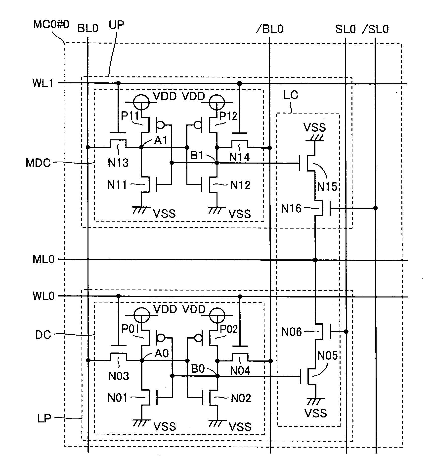
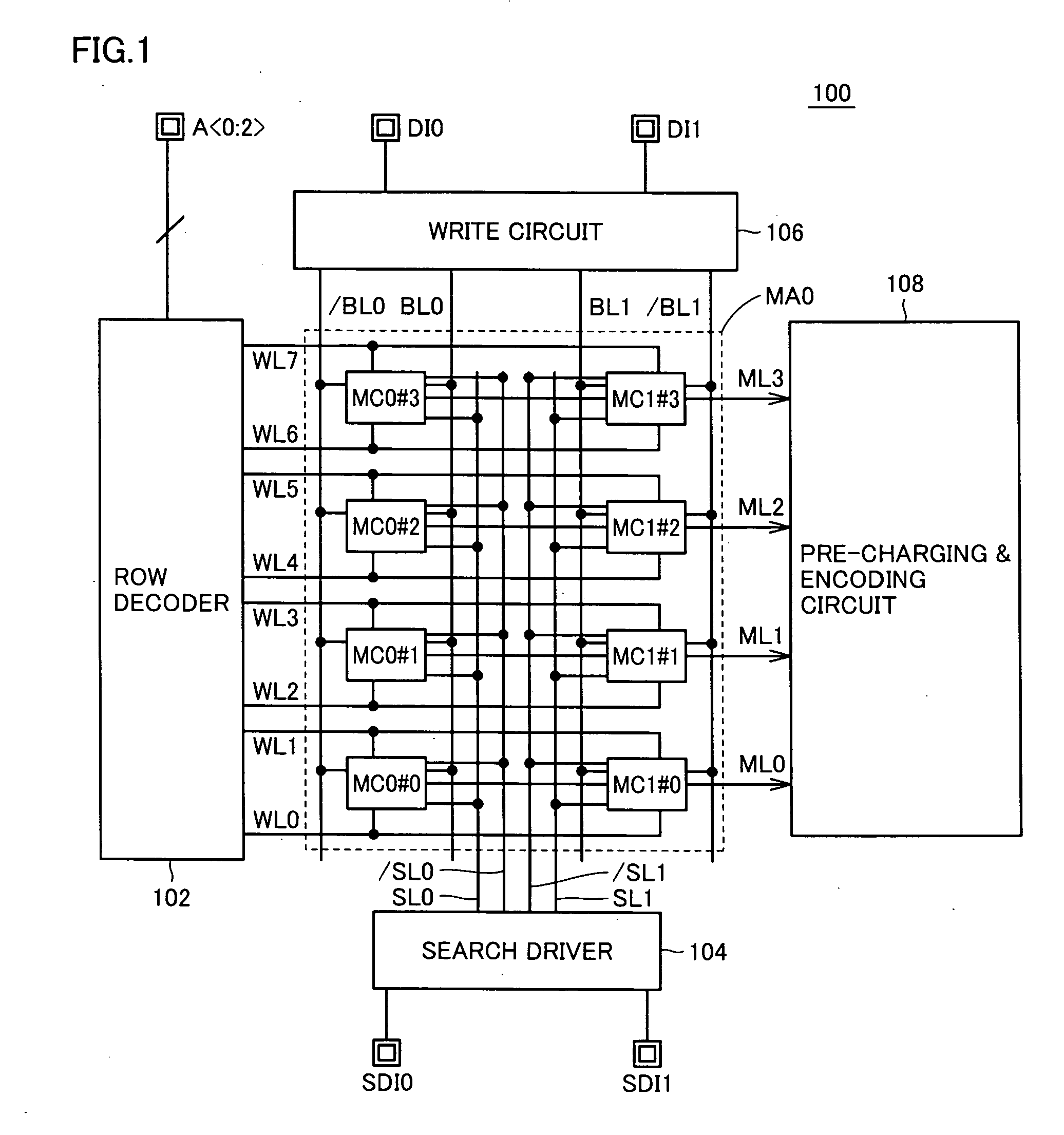
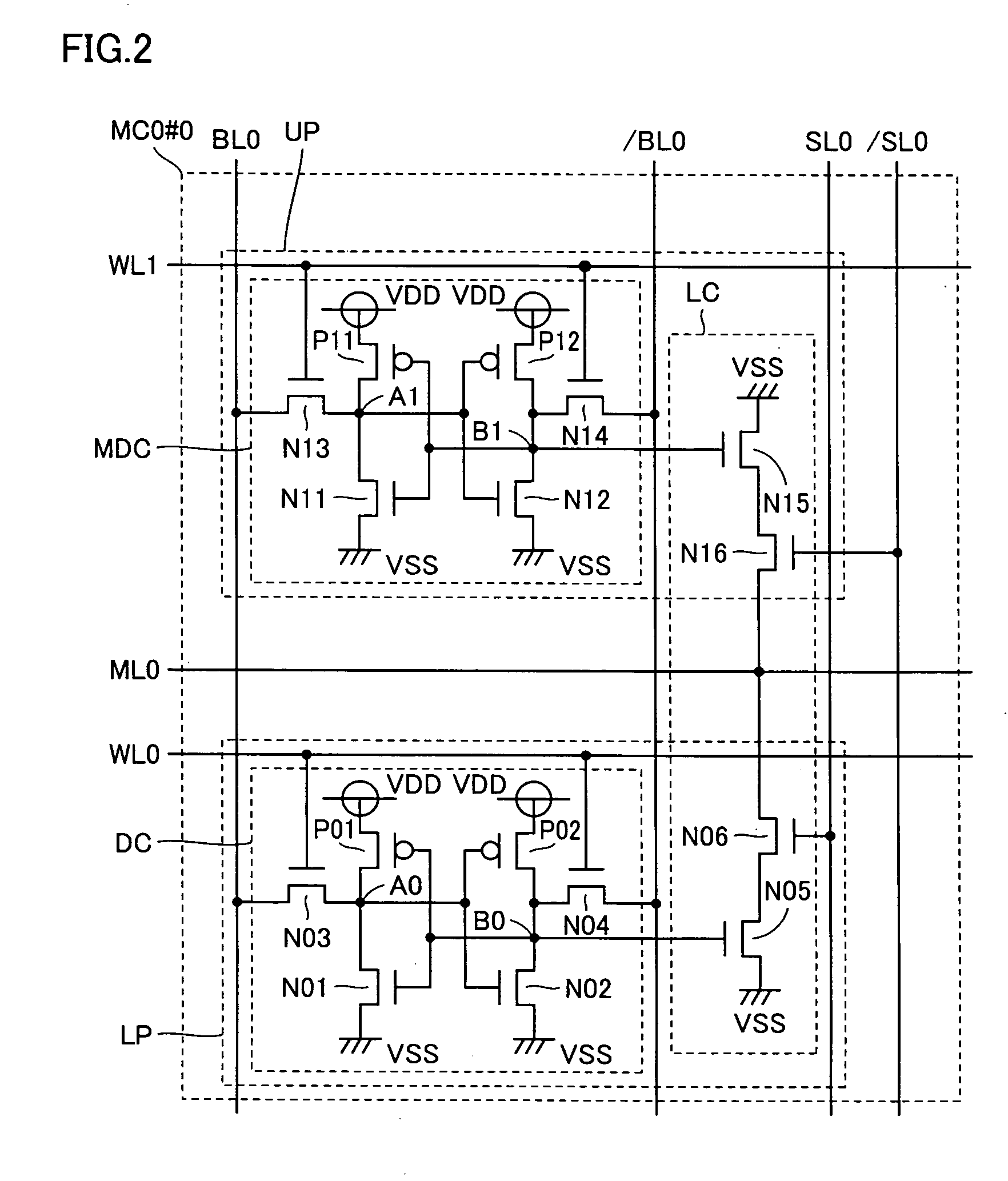
[0041]FIG. 1 is a block diagram schematically showing the configuration of a semiconductor memory device 100 according to the first embodiment.
[0042] With reference to FIG. 1, semiconductor memory device 100 includes: a row decoder 102 receiving an address signal A and activating word lines WL0 to WL7; a write circuit 106 driving bit lines BL0 and / BL0 in response to input data DI0, and driving bit line pair BL1 and / BL1 in response to input data signal DI1; a search driver 104 driving search line pair SL0 and / SL0 in response to a search data signal SDI0, and driving search line pair SL1 and / SL1 in response to a search data signal SDI1; a memory array MA0, to which word lines WL0 to WL7, bit line pairs BL0 and / BL0 as well as BL1 and / BL1, search line pairs SL0 and / SL0 as well as SL1 and / SL1, and match lines ML0 to ML 3 are connected; and a pre-charging & encoding circuit 108 pre-charging match lines ML0 to ML3 and encoding the search results which are outputted to match lines ...
second embodiment
[0130]FIG. 9 is a block diagram schematically showing a semiconductor memory device according to the second embodiment.
[0131] With reference to FIG. 9, a semiconductor memory device 200 includes: a row decoder 202 for selectively activating word lines WL0 to WL3 in response to an address signal A; and a search driver 204 for driving search line pairs SL0 and / SL0 as well as SL1 and / SL1 in response to search data SDI0 and SDI1.
[0132] Semiconductor memory device 200 further includes: a write circuit 206 for driving bit line pairs BL0A and / BL0A, BL0B and / BL0B, BL1A and / BL1A as well as BL1B and / BL1B in response to input data DI0A, DI1A, DI0B and DI1B; a memory array MA1, which are connected to word lines WL0 to WL3, search line pairs SL0 and / SL0, SL1 and / SL1 and bit line pairs BL0A and / BL0A, BL0B and / BL0B, BL1A and / BL1A, BL1B and / BL1B; and a pre-charging & encoding circuit 208 for pre-charging match lines ML0 to ML3, which extend from memory array MA1 and for encoding the co...
third embodiment
[0178] The semiconductor memory device according to the third embodiment has the same circuit configuration and the same arrangement of the cells in the memory array as those shown in FIGS. 9 and 10 of the semiconductor memory device according to the second embodiment, but a different arrangement of the transistors inside the memory cells as well as different interconnection layers for search lines and word lines.
[0179] FIGS. 18 to 21 are plan diagrams showing the internal layout of the memory cells according to the third embodiment. In order to make understanding easier, cross sections along several layers across the entirety, which include the layer where transistors are formed and a plurality of interconnection layers, are shown in the same manner as in the first and second embodiments.
[0180]FIG. 18 is a plan diagram showing the arrangements of a well, a diffusion region DF, polysilicon PO and a contact hole CT of a memory cell according to the third embodiment.
[0181] As can b...
PUM
 Abstract
Description
Claims
Application Information