
Eureka
For R&D, Eureka makes reading and utilizing patents & technical documents easy.
Eureka AIR
Designed for self-driven R&D workflows. Generate viable solutions, solve complex R&D challenges, empower your innovation with AI.

Eureka Materials
Designed for material experts only. Revolutionize your material R&D, from search, analyze, to developing new materials.

TechResearch
Generate reliable direction feasibility study reports for your R&D in just a few steps.

TechSeek
Discover and master advanced knowledge NOW. Basics, ideas, possibilities, all at once.

TechMind
As an expert in R&D Theories, TechMind can generates customized viable solutions instantly.

TechRisk
Analyze your overall solution with one click, know your potential R&D risks in advance.

TechMonitor
Get weekly tech updates, stay abreast of the latest tech innovations and key insights.
CMOS image sensor and manufacturing method thereof
- Summary
- Abstract
- Description
- Claims
- Application Information
AI Technical Summary
Benefits of technology
Problems solved by technology
Method used
Image

Examples
first embodiment
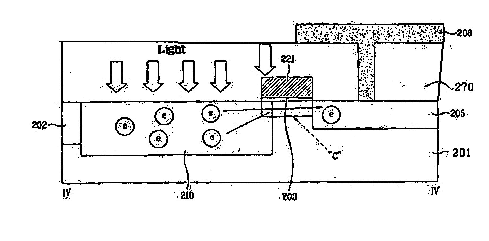
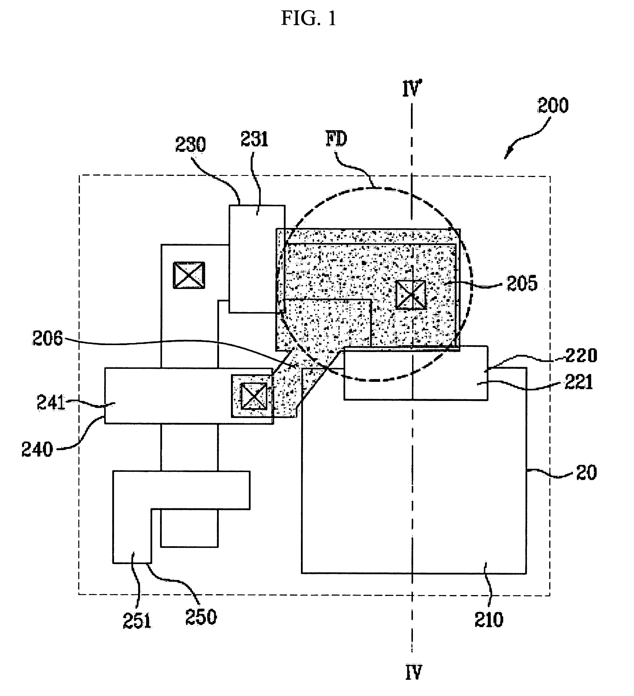
[0018]FIG. 1 is a layout of a CMOS image sensor according to the first embodiment of the present invention, and FIG. 2 is a sectional view of the CMOS image sensor in FIG. 1 taken along line IV-IV′.
[0019] In the first embodiment of the present invention, a 4T-type CMOS image sensor including four transistors per unit pixel is described. However, the first embodiment is not limited to a 4T-type CMOS image, and can include a 3T or a 5T-type CMOS image sensor.
[0020] Referring to FIG. 1, a unit pixel 200 of a CMOS unit sensor, being a photoelectric converter, can be formed in a structure including a photodiode 210 and four transistors. Here, the respective four transistors are a transfer transistor 220, a reset transistor 230, a drive transistor 240, and a select transistor 250.
[0021] The unit pixel 200 of the 4T CMOS image sensor according to the present invention has an active region 20 (defined by the thick line) and a device separating (or isolation) layer formed on or in regions...
second embodiment
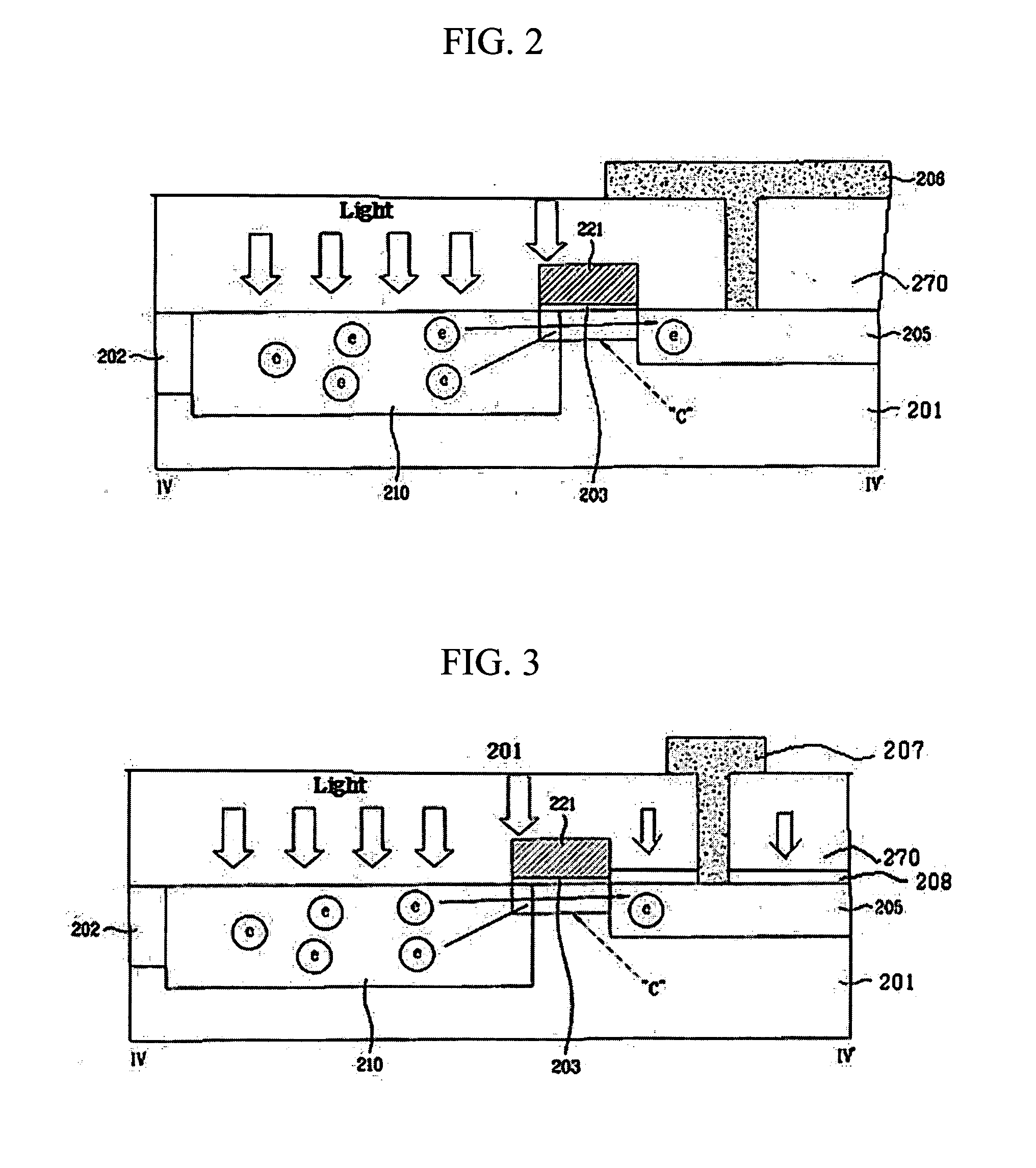
[0032]FIG. 3 is a sectional view of a CMOS image sensor according to the second embodiment of the present invention.
[0033] The second embodiment differs from the first embodiment of the present invention in that an opaque film formed on the transistor region acts as a light blocking agent. That is, metal line 206 in the first embodiment prevent light from being absorbed by the floating diffusion region 205.In the second embodiment, however, an opaque insulating layer 204—for example, silicon nitride (Si3N4)—can be formed on or above the floating diffusion region 205 to block or reduce light from being absorbed by the floating diffusion region 205. At least in the area of the contact hole in insulating layer 270, metal line 207 may also help block light from being absorbed by the floating diffusion region 205.
[0034] The above-described CMOS image sensor according to the present invention has the following advantages.
[0035] First, by blocking the light entering the floating diffusi...
PUM
 Abstract
Description
Claims
Application Information
 - R&D Engineer
- R&D Manager
- IP Professional
- Industry Leading Data Capabilities
- Powerful AI technology
- Patent DNA Extraction
Browse by: Latest US Patents, China's latest patents, Technical Efficacy Thesaurus, Application Domain, Technology Topic, Popular Technical Reports.
© 2024 PatSnap. All rights reserved.Legal|Privacy policy|Modern Slavery Act Transparency Statement|Sitemap|About US| Contact US: help@patsnap.com