Tape wiring substrate and chip-on-film package using the same

a technology of wiring substrate and chip-on-film package, which is applied in the direction of printed circuit aspects, cross-talk/noise/interference reduction, basic electric elements, etc., can solve the problems of poor electromagnetic interference and/or noise characteristics, and the cof package b>100/b> may unstably supply power to the semiconductor chip

Active Publication Date: 2007-01-18
SAMSUNG ELECTRONICS CO LTD
View PDF6 Cites 32 Cited by
  • Summary
  • Abstract
  • Description
  • Claims
  • Application Information

AI Technical Summary

Problems solved by technology

The conventional COF package 100 may insufficiently reduce electromagnetic waves and / or noise that may occur during operation of the semiconductor chip 10, which may result in poor electromagnetic interference and / or noise characteristics.
Further, the conventional COF package 100 may unstably supply power to the semiconductor chip 10.

Method used


Image

  • Tape wiring substrate and chip-on-film package using the same
  • Tape wiring substrate and chip-on-film package using the same
  • Tape wiring substrate and chip-on-film package using the same

Examples


Embodiment Construction

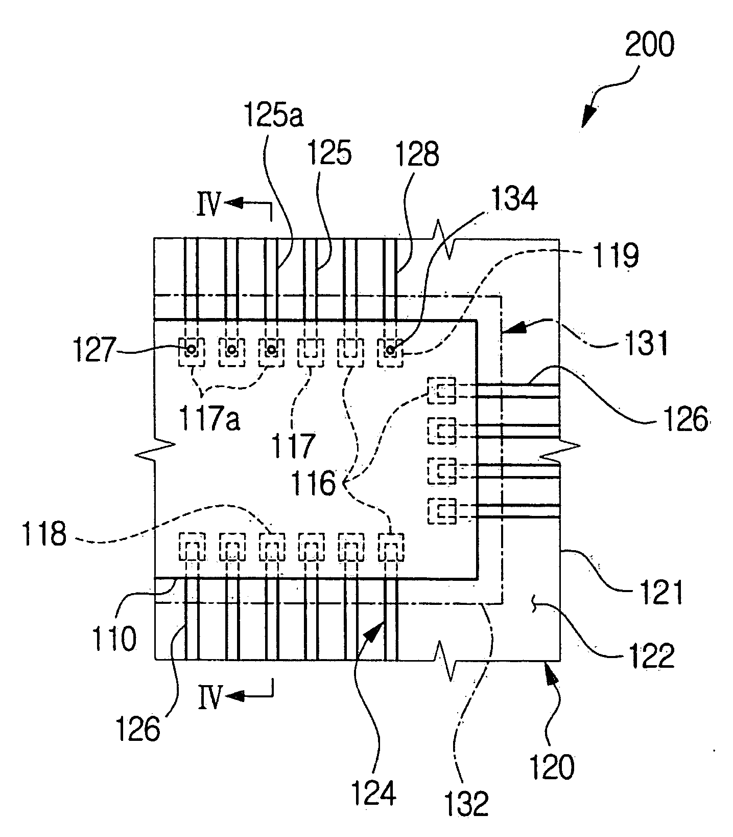
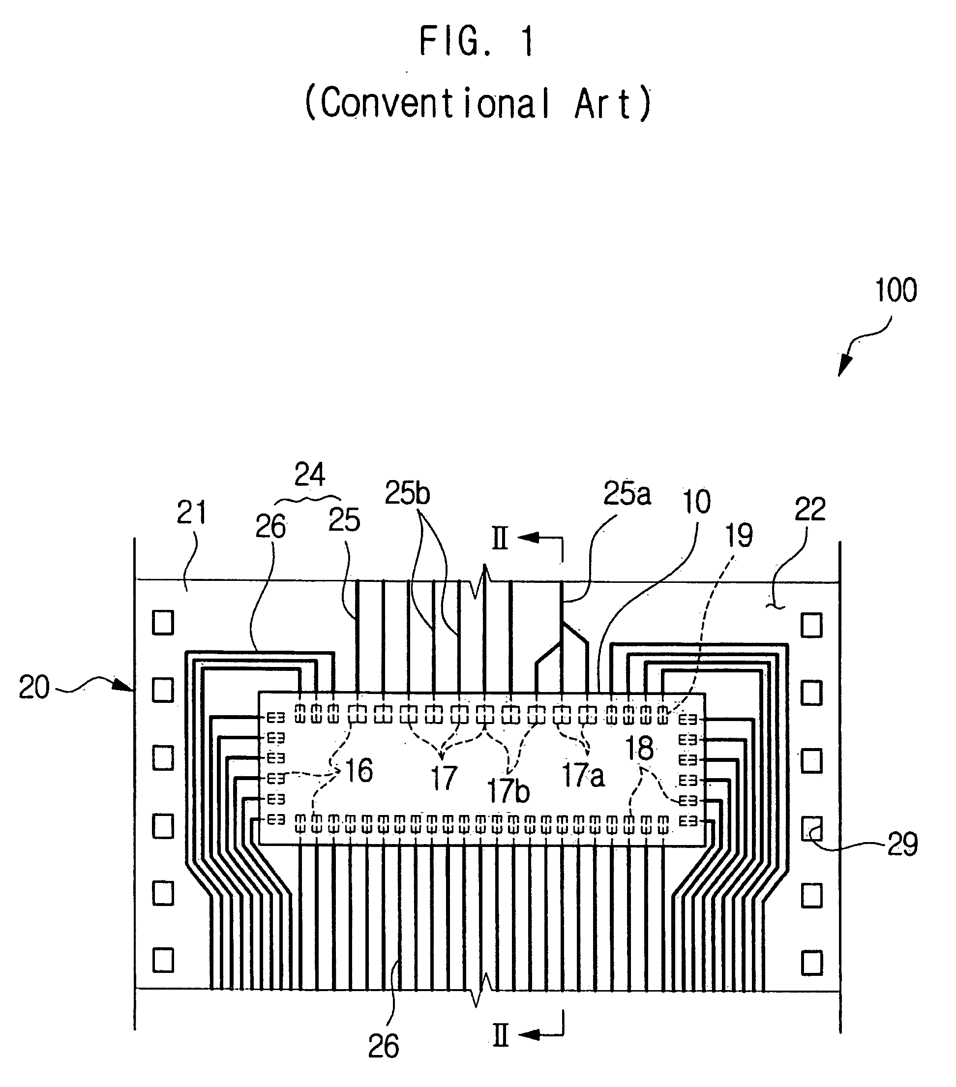
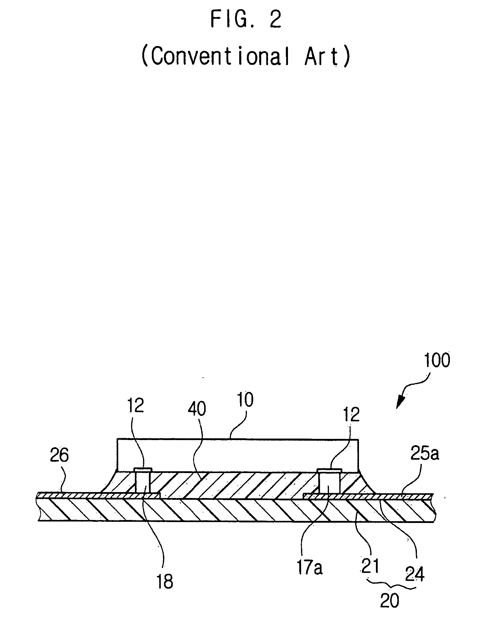
[0029] Example, non-limiting embodiments of the present invention will be described more fully with reference to the accompanying drawings. This invention may, however, be embodied in many different forms and should not be construed as limited to the example embodiments set forth herein. Rather, the disclosed embodiments are provided so that this disclosure will be thorough and complete, and will fully convey the scope of the invention to those skilled in the art. The principles and features of this invention may be employed in varied and numerous embodiments without departing from the scope of the invention.

[0030] An element is considered as being mounted (or provided) “on” another element when mounted or provided) either directly on the referenced element or mounted (or provided) on other elements overlaying the referenced element. Throughout this disclosure, spatial terms such as “upper,”“lower,”“above” and “below” (for example) are used for convenience in describing various ele...


PUM


Abstract

A chip-on-film package may include a tape wiring substrate, a semiconductor chip mounted on the tape wiring substrate, and a molding compound provided between the semiconductor chip and the tape wiring substrate. The tape wiring substrate may include a film having upper and lower surfaces. Vias may penetrate the film. An upper metal layer may be provided on the upper surface of the film and include input terminal patterns and/or output terminal patterns. The input terminal patterns may include ground terminal patterns and/or power terminal patterns. A lower metal layer may be provided on the lower surface of the film and include a ground layer and/or a power layer. The ground layer and the power layer may cover at least a chip mounting area.

Description

PRIORITY STATEMENT [0001] This U.S. non-provisional application claims benefit of priority under 35 U.S.C. §119 from Korean Patent Application No. 2005-64789, filed on Jul. 18, 2005, the entire contents of which are incorporated herein by reference. BACKGROUND [0002] 1. Field of the Invention [0003] Example embodiments of the present invention relate in general to a tape wiring substrate and a tape package using the tape wiring substrate and, more particularly, to a tape wiring substrate that may have a dual metal layer and a chip-on-film package that may implement the tape wiring substrate. [0004] 2. Description of the Related Art [0005] Flat panel displays may include, for example, a liquid crystal display (“LCD”) for portable phones, a thin-film transistor liquid crystal display (“TFT LCD”) for computers and plasma display panels (“PDP”) for domestic use. A flat panel display may include a component part known in the art as a tape package. In some applications, the tape package m...

Claims


Application Information

Patent Timeline
Patent Type & Authority Applications(United States)
IPC IPC(8): H01L23/34
CPCH01L23/36H01L23/3677H01L2224/73204H01L2224/32225H01L2224/16225H01L23/49838H01L23/4985H01L23/50H01L23/552H01L24/17H01L2224/13099H01L2924/01015H01L2924/01029H01L2924/01033H01L2924/01079H01L2924/01082H05K1/0216H05K1/113H05K1/189H05K2201/0715H05K2201/09318H01L2924/01006H01L2924/014H01L2924/00H01L2224/05571H01L2224/05573H01L2224/06135H01L2924/00014H01L2924/181H01L2224/05599H01L23/12H01L23/48
Inventor LEE, SI-HOONSONG, EUN-SEOK
Owner SAMSUNG ELECTRONICS CO LTD
Why Eureka
Try Eureka