Multi-layer printed circuit board

Inactive Publication Date: 2007-01-25
HON HAI PRECISION IND CO LTD
View PDF8 Cites 108 Cited by
  • Summary
  • Abstract
  • Description
  • Claims
  • Application Information

AI Technical Summary

Problems solved by technology

Additionally, currents running through the vias gene

Method used


Image

  • Multi-layer printed circuit board
  • Multi-layer printed circuit board

Examples


Embodiment Construction

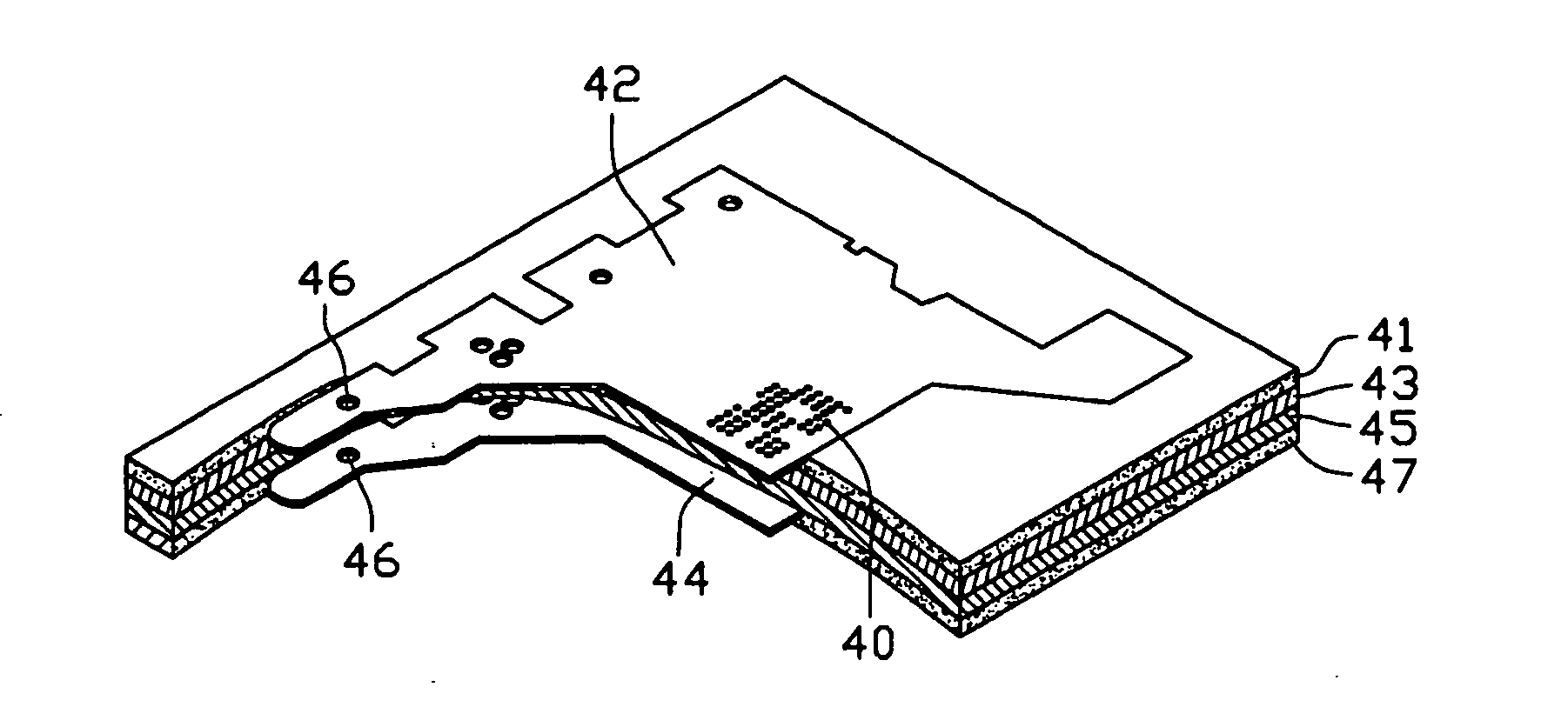
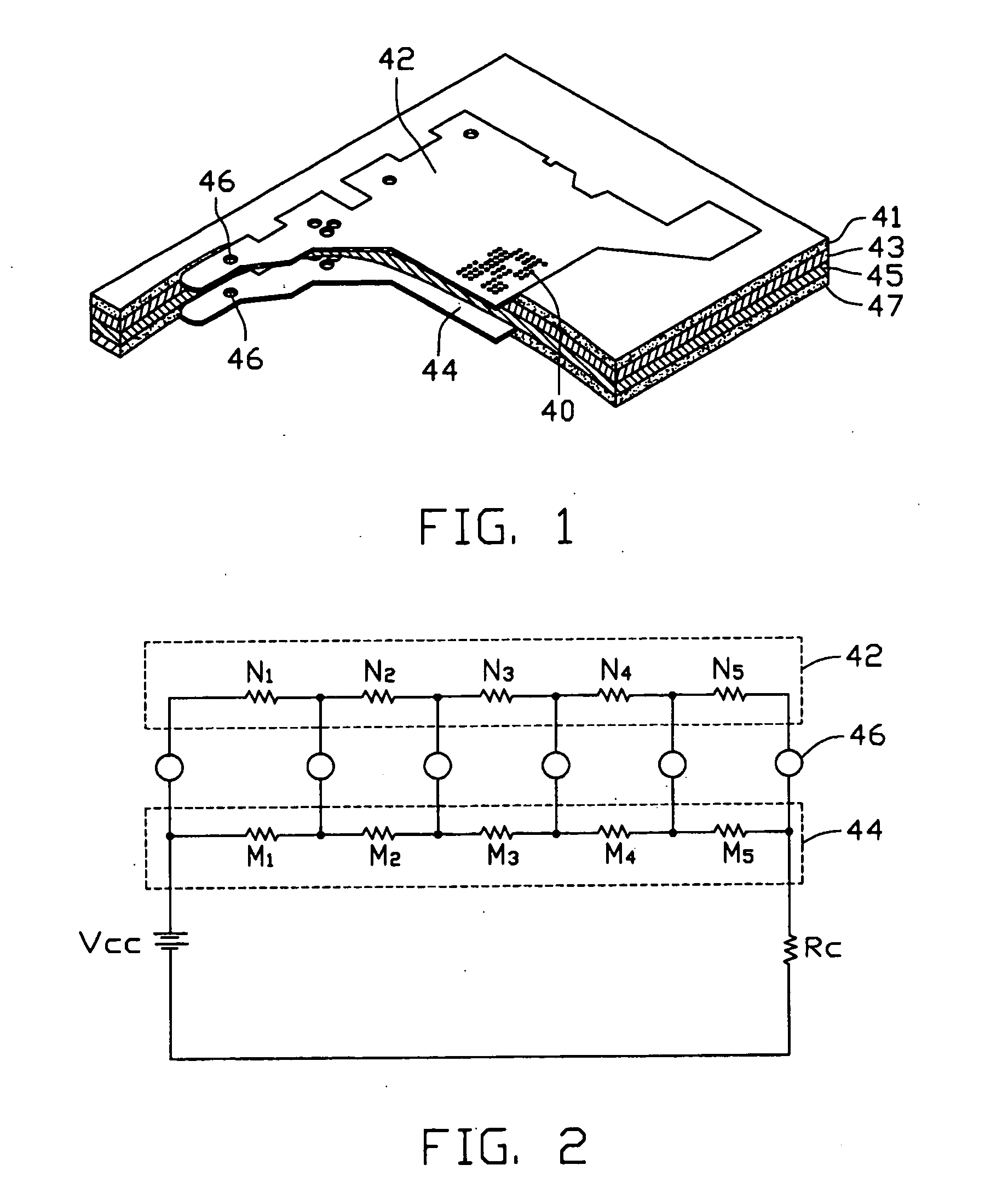
[0010] Referring to FIG. 1, a circuit assembly like a multi-layer printed circuit board (PCB) in accordance with a preferred embodiment of the present invention includes a first signal layer 41, a ground layer 43, a power layer 45, and a second signal layer 47 disposed sequentially one above the other. The first signal layer 41 includes a first power area 42. The first power area 42 includes a plurality of pads 40, for mounting a component requiring large working current thereon. The second signal layer 47 includes a second power area 44, cooperating with the first power area 42 to provide power to the component. A plurality of vias 46 is correspondingly defined in the first power area 42 and the second power area 44, electrically connecting the first power area 42 to the second power area 44. The vias 46 also extend through the ground layer 43 and the power layer 45 of the PCB. In the preferred embodiment, one of the pads 40 electronically connects with one of the vias 46 to provid...


PUM


Abstract

A multi-layer printed circuit board (PCB) is provided allowing balanced power supply to components requiring large working current. The PCB includes a plurality of layers disposed thereon. A first power area, and a second power area are separately arranged on different layers. The first power area and the second power area vertically aligned within the PCB with generally identical shapes cooperatively provide power to components requiring large working current.

Description

BACKGROUND [0001] 1. Field of the Invention [0002] The present invention relates to multi-layer printed circuit boards (PCBs), and more particularly to a multi-layer PCB which is capable of providing a balanced power supply to a component requiring large working current and efficiently maintaining PCB integrity. [0003] 2. General Background [0004] Conventionally, components requiring large working currents (such as central processing units (CPUs), Voltage Regulator Modules (VRMs), North Bridge Chips (NBCs), and memories mounted on PCBs often require dual power areas provided by a power supply. The dual power areas with identical voltages are typically disposed in two different layers (such as a power layer and a signal layer) and are connected in parallel. However, the dual power areas with different sizes and shapes will have different impedances. As a result, the dual power areas separately consume different amounts of voltages thus providing different voltages to the component. T...

Claims


Application Information

Patent Timeline
IPC IPC(8): H05K1/11
CPCH05K1/0265H05K2201/0979H05K2201/093H05K1/115
Inventor LIN, YU-HSUYEH, SHANG-TSANGHUANG, CHAO-CHENLI, CHUAN-BING
Owner HON HAI PRECISION IND CO LTD
Why Eureka
Try Eureka