Apparatus for feature detection

a technology for feature detection and apparatus, applied in the field of apparatus for feature detection of test objects, can solve the problems of high production cost, inflexible configuration of illumination system, and the inability of control device to successfully verify the features of printed circuit boards

Inactive Publication Date: 2007-01-25
CHROMA ATE
View PDF3 Cites 44 Cited by
  • Summary
  • Abstract
  • Description
  • Claims
  • Application Information

AI Technical Summary

Benefits of technology

[0009] Therefore, the object of the present invention is to provide an apparatus for feature detection that can overcome at least one of the aforesaid drawbacks of the prior art.

Problems solved by technology

For example, if an electric component on the printed circuit board has a shiny surface that reflects light away from the image capturing module, the image capturing module would not be able to receive the reflected light from the electric component, and the area where the electric component is supposed to be in would appear black in the images captured by the image capturing module, thereby preventing the control device from successfully verifying the features of the printed circuit board.
While the illumination system in WO 02 / 01210 A1 permits illumination of a test region from different angles or from different combinations of angles, formation of the serrations involves complex and precise manufacturing processes and equipment, which result in high production costs.
In addition, such an illumination system cannot be flexibly configured.

Method used


Image

  • Apparatus for feature detection
  • Apparatus for feature detection
  • Apparatus for feature detection

Examples


Embodiment Construction

[0018] Before the present invention is described in greater detail with reference to the accompanying preferred embodiments, it should be noted herein that like elements are denoted by the same reference numerals throughout the disclosure.

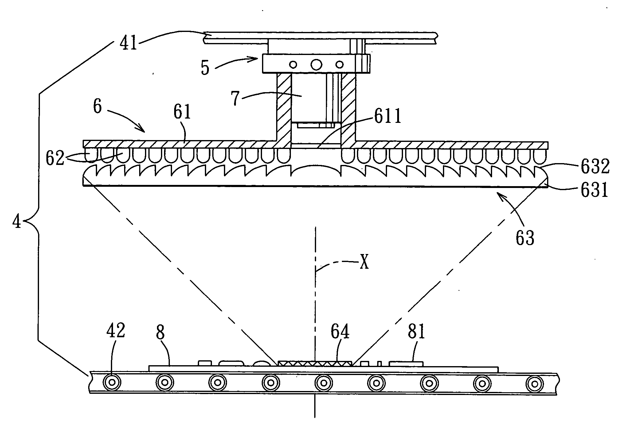
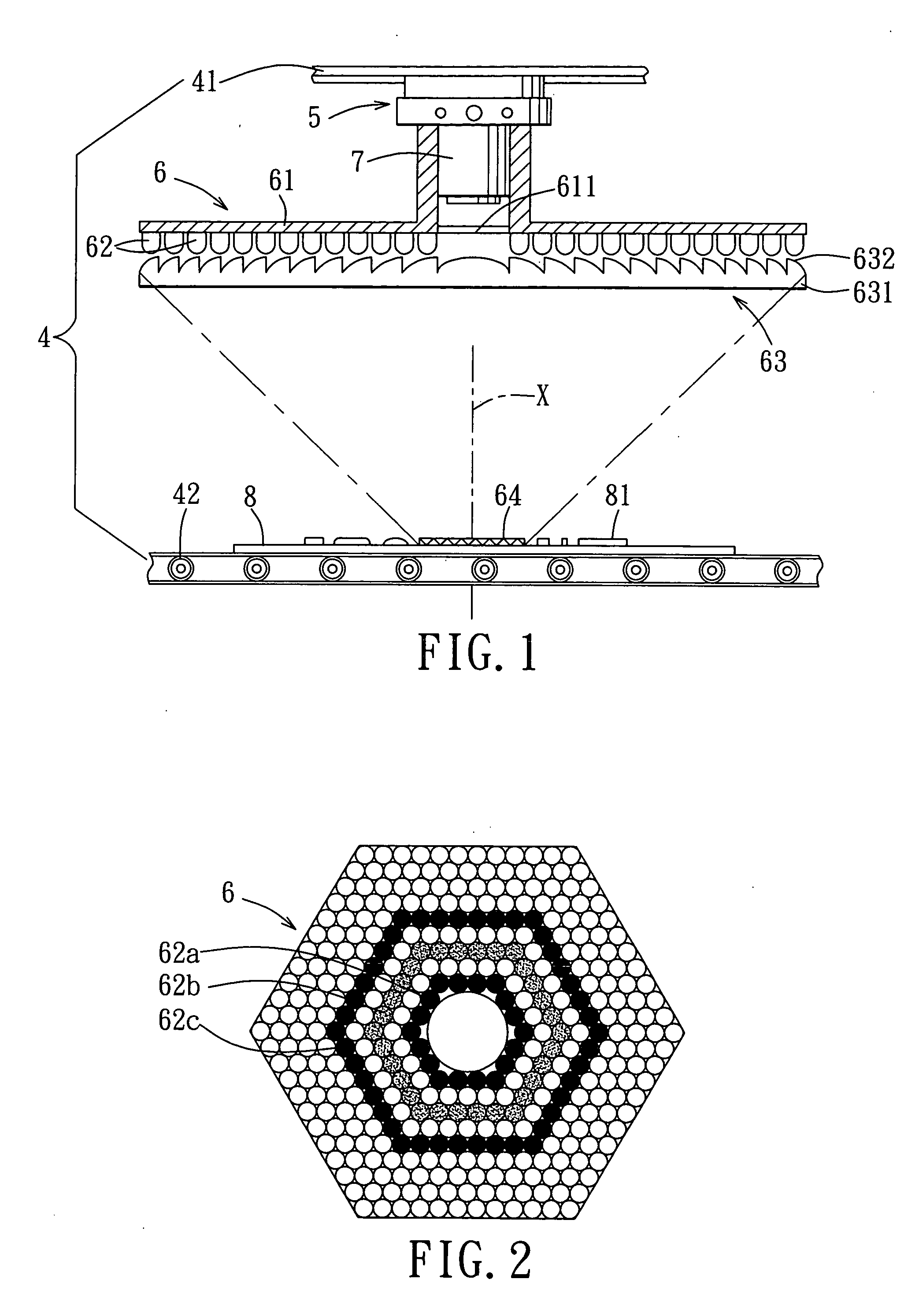
[0019] Referring to FIG. 1, the first preferred embodiment of an apparatus for feature detection according to the present invention is shown to be adapted for inspecting a surface of a test object 8 in order to collect and analyze two-dimensional features of the test object 8. The surface of the test object 8 is perpendicular to a reference line (X) . In this embodiment, the test object 8 is exemplified as a printed circuit board having electric components 81, such as capacitors, resistors, integrated circuits, etc., mounted on a surface thereof. The apparatus includes a moving module 4, a control module 5, a light source module 6, and an image capturing unit 7.

[0020] The moving module 4 is used to generate relative movement of the control module...


PUM

PropertyMeasurementUnit
distanceaaaaaaaaaa
response timeaaaaaaaaaa
colorsaaaaaaaaaa

Abstract

An apparatus for feature detection of a test object includes at least one light source module and at least one image capturing unit. The light source module provides light to illuminate a test region of the test object, and includes a substrate, a set of light-emitting components, and a light-focusing unit. The light-emitting components are mounted on the substrate for emitting light in parallel directions that are generally transverse to the substrate. The light-focusing unit is to be disposed between the light-emitting components and the test object, receives the light emitted by the light-emitting components, and focuses the light on the test region of the test object. The image capturing unit captures an image of the test object at the test region.

Description

BACKGROUND OF THE INVENTION [0001] 1. Field of the Invention [0002] The invention relates to an apparatus for feature detection of a test object, more particularly to a simple and low cost apparatus for feature detection of a test object. [0003] 2. Description of the Related Art [0004] Automated optical inspection is used during the manufacture of printed circuit boards and the like. During an automated surface mounting process, an automated optical inspection system is used to verify features of mounted electric components. A conventional automated optical inspection system generally includes an image capturing device to be disposed above a target printed circuit board and operable so as to capture images of test regions of the target printed circuit board, a moving device for generating relative movement between the image capturing device and the target printed circuit board, and a computerized control device for controlling the operation of the moving device and for analyzing the...

Claims


Application Information

Patent Timeline
Patent Type & Authority Applications(United States)
IPC IPC(8): G01N21/88
CPCG01N21/8806G01N2021/95638G01N2021/8845G01N21/95684
Inventor SUNG, HSIN-YUEHCHUNG, BING-SHIENLO, WEN-CHILIAO, CHIN-CHIANGLIU, MIAO-SHEN
Owner CHROMA ATE
Why Eureka
Try Eureka