Small thin film movable element, small thin film movable element array and method of driving small thin film movable element array

a technology of small thin film and array, applied in static indicating devices, instruments, optics, etc., to achieve the effect of high speed formation and shortening a time period

Inactive Publication Date: 2007-02-01
FUJIFILM CORP +1
View PDF4 Cites 19 Cited by
  • Summary
  • Abstract
  • Description
  • Claims
  • Application Information

AI Technical Summary

Benefits of technology

[0012] The invention has been carried out in view of the above-described situation and it is an object thereof to provide a small thin film movable element and a small thin film movable element array as well as a method of driving a small thi...

Problems solved by technology

According to the small thin film movable element, an excessive electrostatic force produced by applying a voltage larger than the static pull-in voltage is not generated, further, a deficiency in t...

Method used


Image

  • Small thin film movable element, small thin film movable element array and method of driving small thin film movable element array
  • Small thin film movable element, small thin film movable element array and method of driving small thin film movable element array
  • Small thin film movable element, small thin film movable element array and method of driving small thin film movable element array

Examples


first embodiment

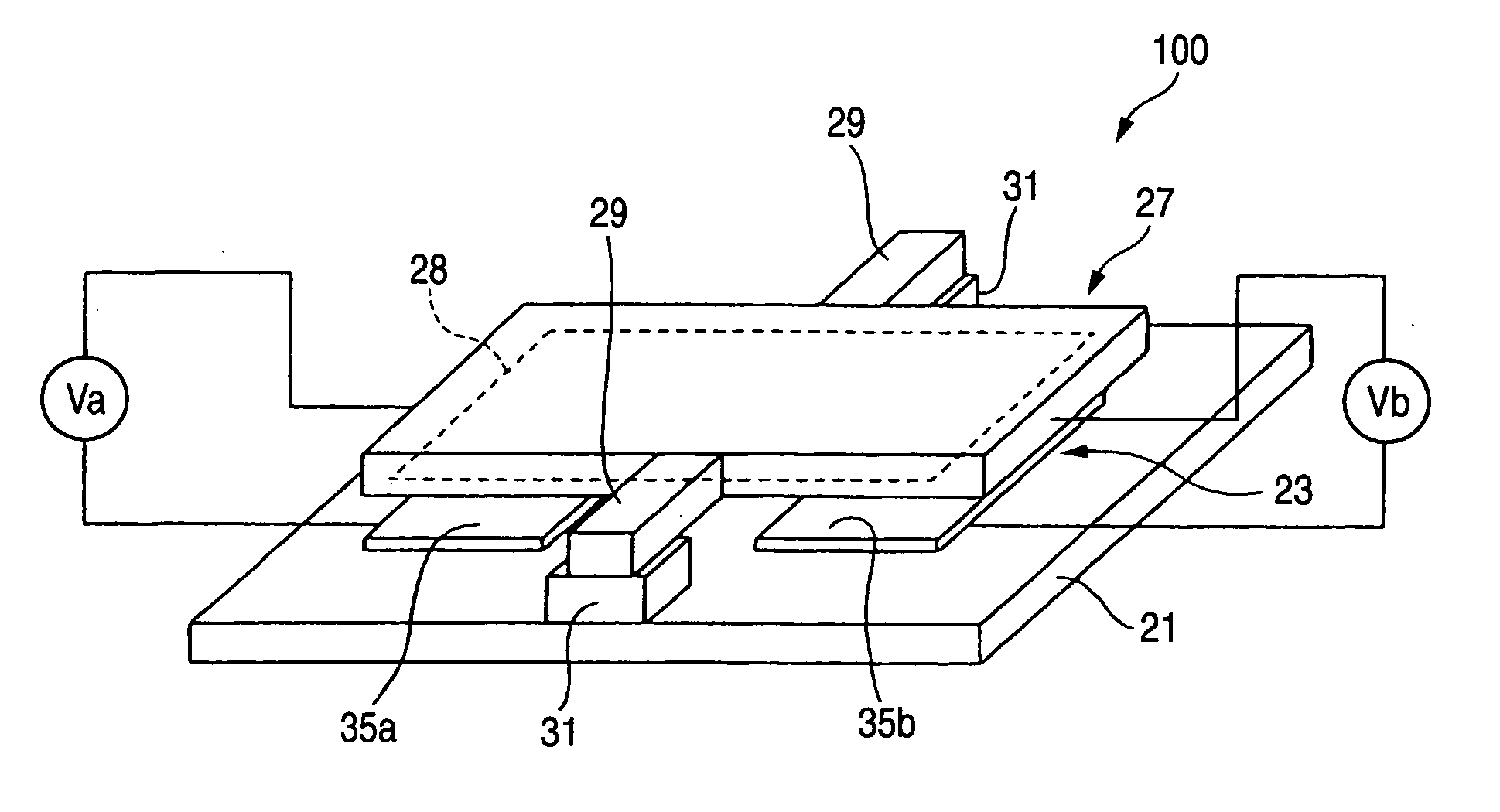
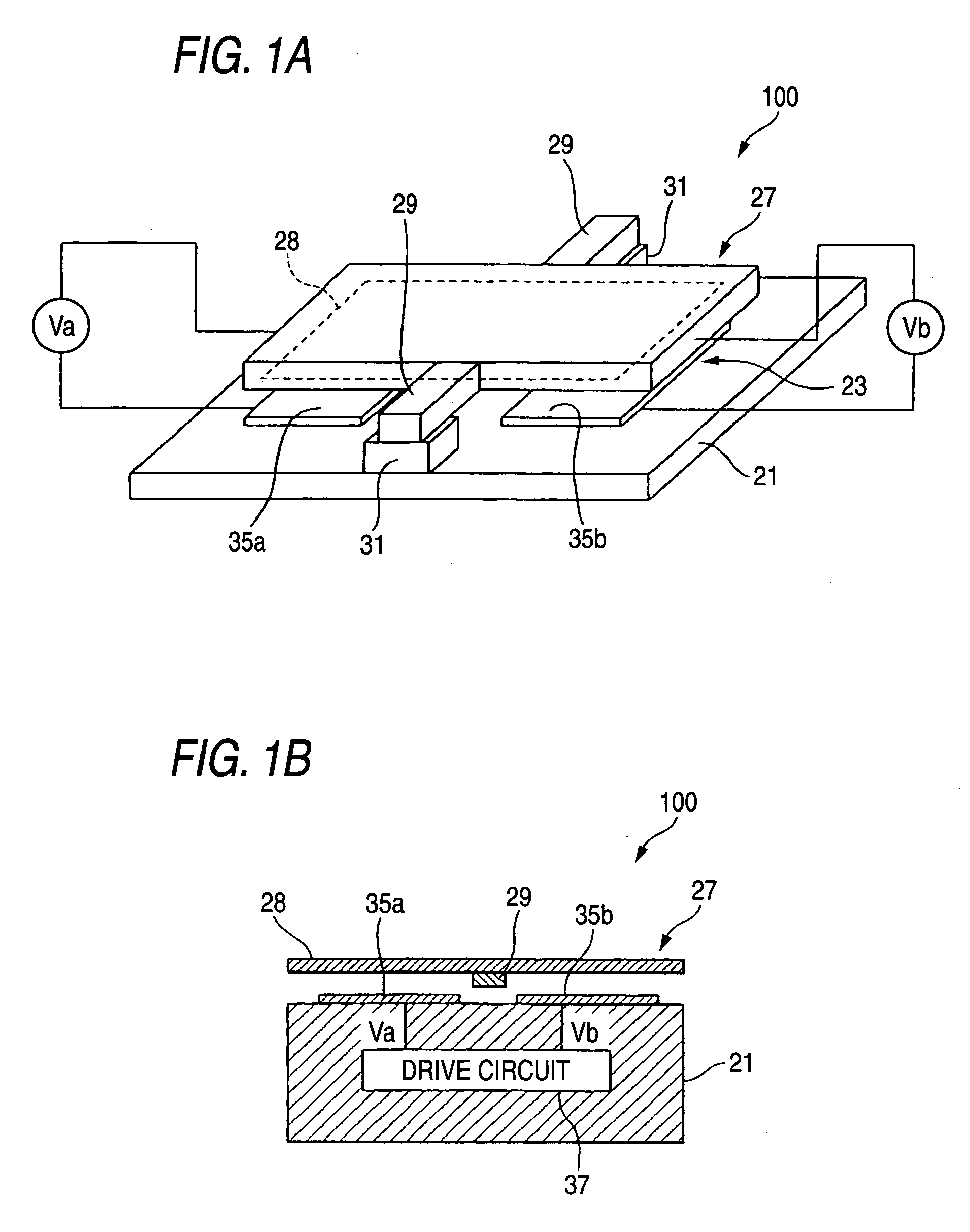
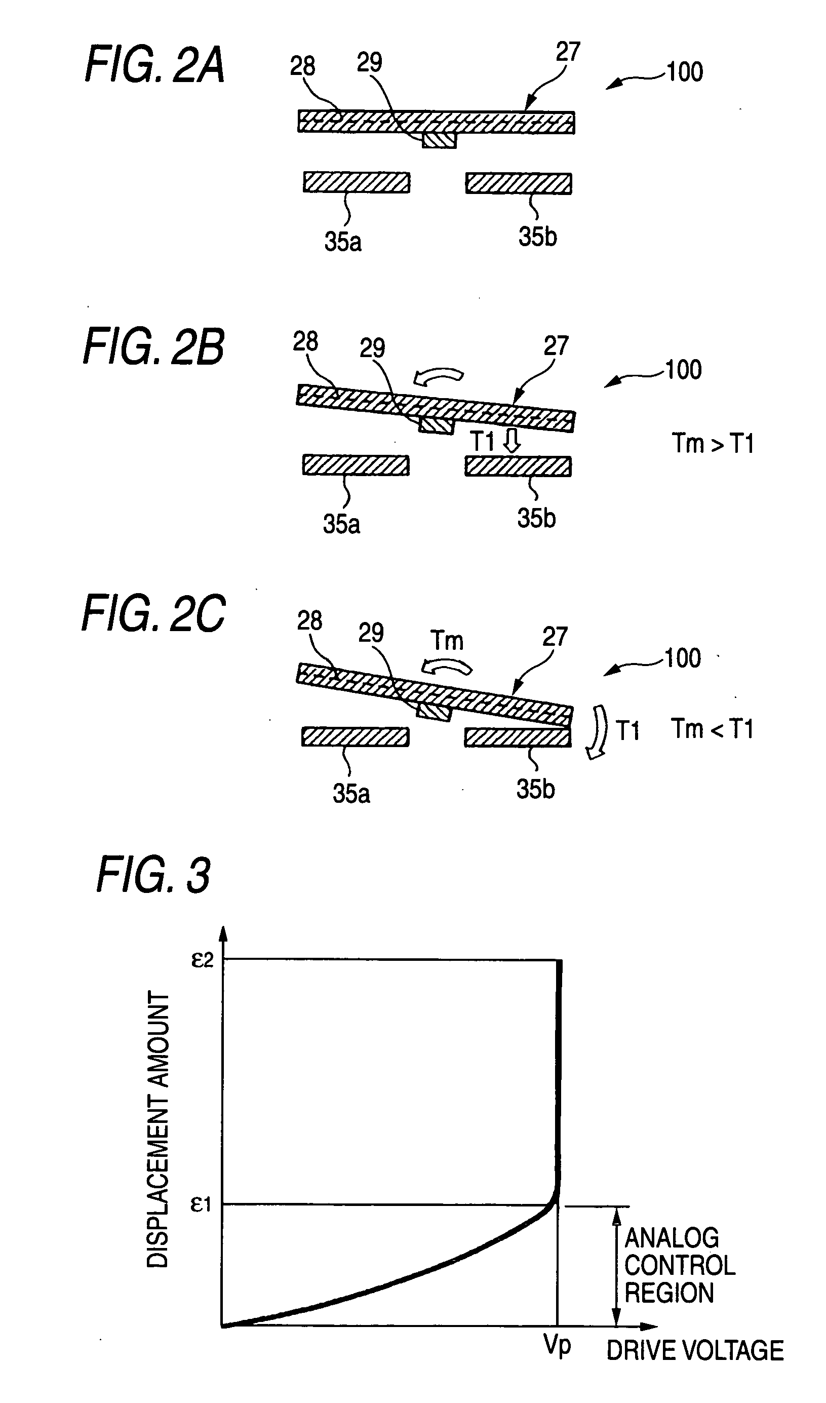
[0067]FIGS. 1A and 1B illustrate conceptual views showing a small thin film movable element according to the invention, FIGS. 2A to 2C illustrate explanatory views of operation showing an operational procedure in applying a static pull-in voltage of the small thin film movable element shown in FIG. 1, FIG. 3 is an explanatory view showing a correlation between a displacement amount and a drive voltage operated to a movable portion in applying the static pull-in voltage, and FIGS. 4A to 4C illustrate explanatory views of operation showing an operational procedure in applying a dynamic pull-in voltage of the small thin film movable element shown in FIG. 1.

[0068] A small thin film movable element 100 according to the embodiment includes a movable portion 27 in a shape of a small piece arranged in parallel with a board 21 by way of a gap 23, hinges 29, 29 constituting support portions extended from both edge portions of the movable portion 27, and spacers 31, 31 for supporting the movab...

second embodiment

[0141] Next, a small thin film movable element according to the invention will be explained.

[0142]FIG. 20 illustrates conceptual views showing a second embodiment of a small thin film movable element according to the invention.

[0143] According to a small thin film movable element 200 according to the embodiment, one end of a movable portion 51 is supported to be fixed by the board 21 by way of the hinges 29, 29, the spacer 31, 31. That is, the movable portion 51 is constituted by a shape of a cantilever constituting a free end by other end thereof. Further, the first address electrode 35a is provided on the board 21 to be opposed to the free end of the movable portion 51, and an opposed side of the first address electrode 35a interposing the movable portion 51 is provided with the second address electrode 35b formed at an opposed board, not illustrated.

[0144] Also in the small thin film movable element 200 having such a constitution, the voltage Va, Vb applied between the first ad...

third embodiment

[0145] Next, a small thin film movable element according to the invention will be explained.

[0146]FIGS. 21A and 21B illustrate conceptual views showing a third embodiment of a small thin film movable element according to the invention.

[0147] A small thin film movable element 300 according to the embodiment is an element of a so-to-speak parallel flat plate type, and both ends of a movable portion 61 in a flat plate shape having a conductivity and a flexibility are fixed to an insulating film 63 formed on the board 21 by way of the predetermined gap 23. A lower side of the movable portion 61 of the board 21 is arranged with the first address electrode 35a by way of the insulating film 63, further, an upper side of the movable portion 61 is arranged with the second address electrode 35b by way of an insulating film 65. That is, the movable portion 61 is constituted by a shape of a both support beam both ends of which are supported between the first address electrode 35a and the secon...


PUM


Abstract

A small thin film movable element comprises; a movable portion supported elastically deformably and having a movable electrode at at least a portion of the movable portion; and a fixed electrode arranged to be opposed to the movable portion, wherein the movable portion is displaced by an electrostatic force in accordance with a voltage applied to the movable electrode and the fixed electrode, and wherein the voltage applied in displacing the movable portion falls in a range equal to or lower than a static pull-in voltage for bringing the movable portion into contact with a side of the fixed electrode against a resistance force generated in accordance with an amount of displacing the movable portion and equal to or higher than a minimum dynamic pull-in voltage for bringing the movable portion into contact with the side of the fixed electrode by being compounded with an inertia force generated in accordance with an operation of the movable portion.

Description

BACKGROUND OF THE INVENTION [0001] 1. Field of the Invention [0002] The present invention relates to a small thin film movable element and a small thin film movable element array as well as a method of driving a small thin film movable element array for displacing a movable portion by an electrostatic force in according with a voltage applied to a movable electrode and a fixed electrode, which is preferably used in, for example, optical communication, an exposing apparatus, a projector, an optical switch, a scanner, an RF switch, an actuator, a multiplexor or the like. [0003] 2. Description of the Related Art [0004] In recent years, by rapid progress of an MEMS technology (HEMS; Micro-Electro Mechanical Systems), there has been intensively carried out development of a small thin film movable element for electrically displacing / moving a small thin film of μm order. As the small thin film movable element, there are, for example, a digital micromirror device (DMD) for deflecting light ...

Claims


Application Information

Patent Timeline
IPC IPC(8): G02B26/00
CPCG02B26/0841
Inventor MOCHIZUKI, FUMIHIKOOGIKUBO, SHINYANAKAMURA, HIROCHIKA
Owner FUJIFILM CORP
Why Eureka
Try Eureka