

Film deposition apparatus and film deposition method
a film deposition apparatus and film technology, applied in the field of film deposition apparatus and film deposition method, can solve the problems of reducing the utilization rate productivity, affecting the efficiency of film deposition apparatus, and long process time, so as to reduce the amount of btbas gas adsorption on the wafer w, the effect of reducing the concentration of btbas gas and increasing the throughpu
- Summary
- Abstract
- Description
- Claims
- Application Information
AI Technical Summary
Benefits of technology
Problems solved by technology
Method used
Image

Examples
Embodiment Construction
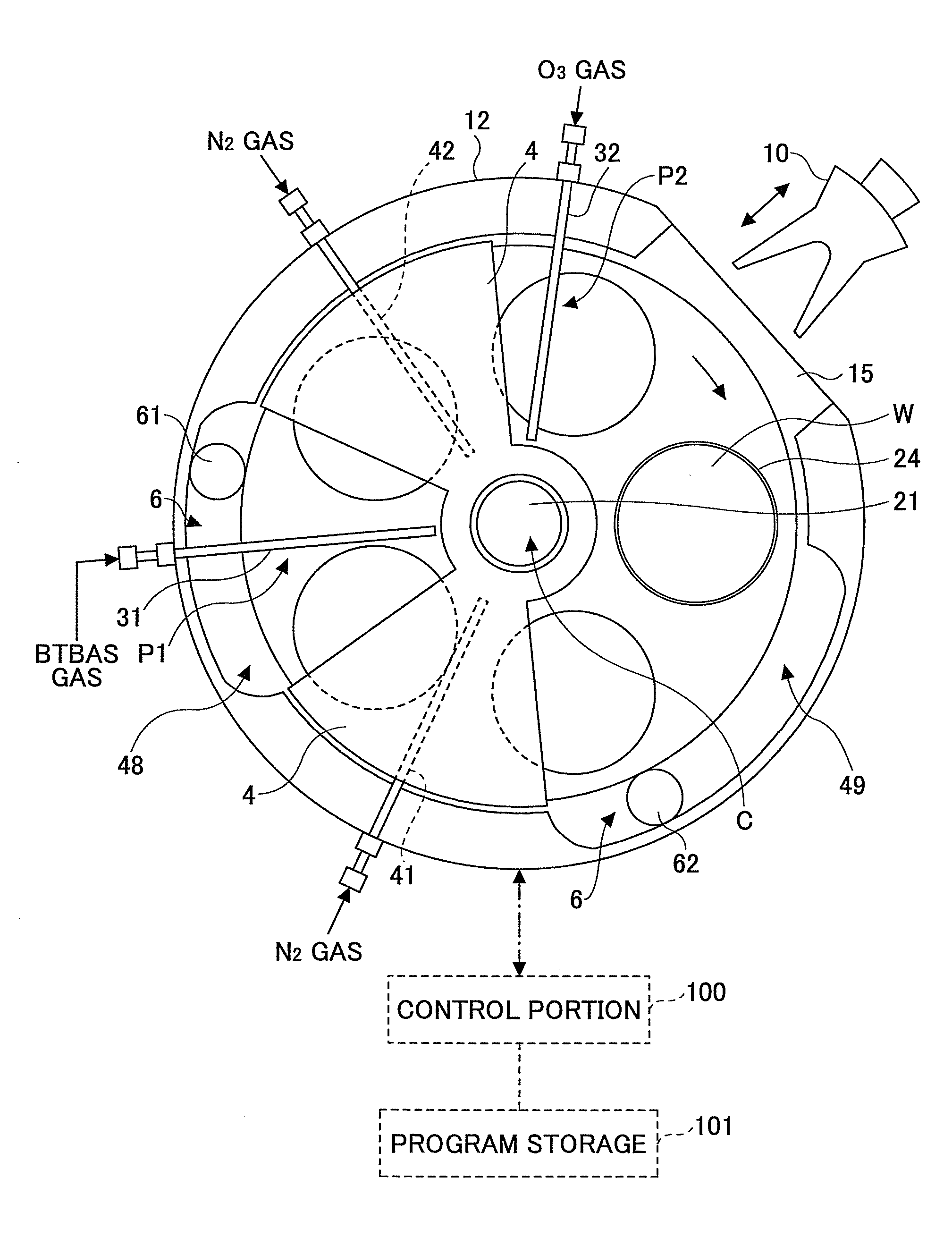
[0084]According to an embodiment of the present invention, a wafer placed in a wafer receiving area of a turntable is substantially prevented from being thrown outward from the wafer receiving area even when the turntable is rotated at relatively high rotation speed, and thus the wafer is substantially prevented from being broken or chipped.
[0085]In addition, according to an embodiment of the present invention, the wafer is substantially prevented from moving or vibrating in the concave portion, while such moving or vibrating may cause breakage and / or chipping of the wafer.
[0086]Therefore, particle generation is substantially avoided, and the ALD is carried out in a clean environment, thereby fully reducing contamination of the wafer and auto-doping of impurities into a film. As a result, the number of reject wafers can be reduced, thereby contributing to improved production yield.
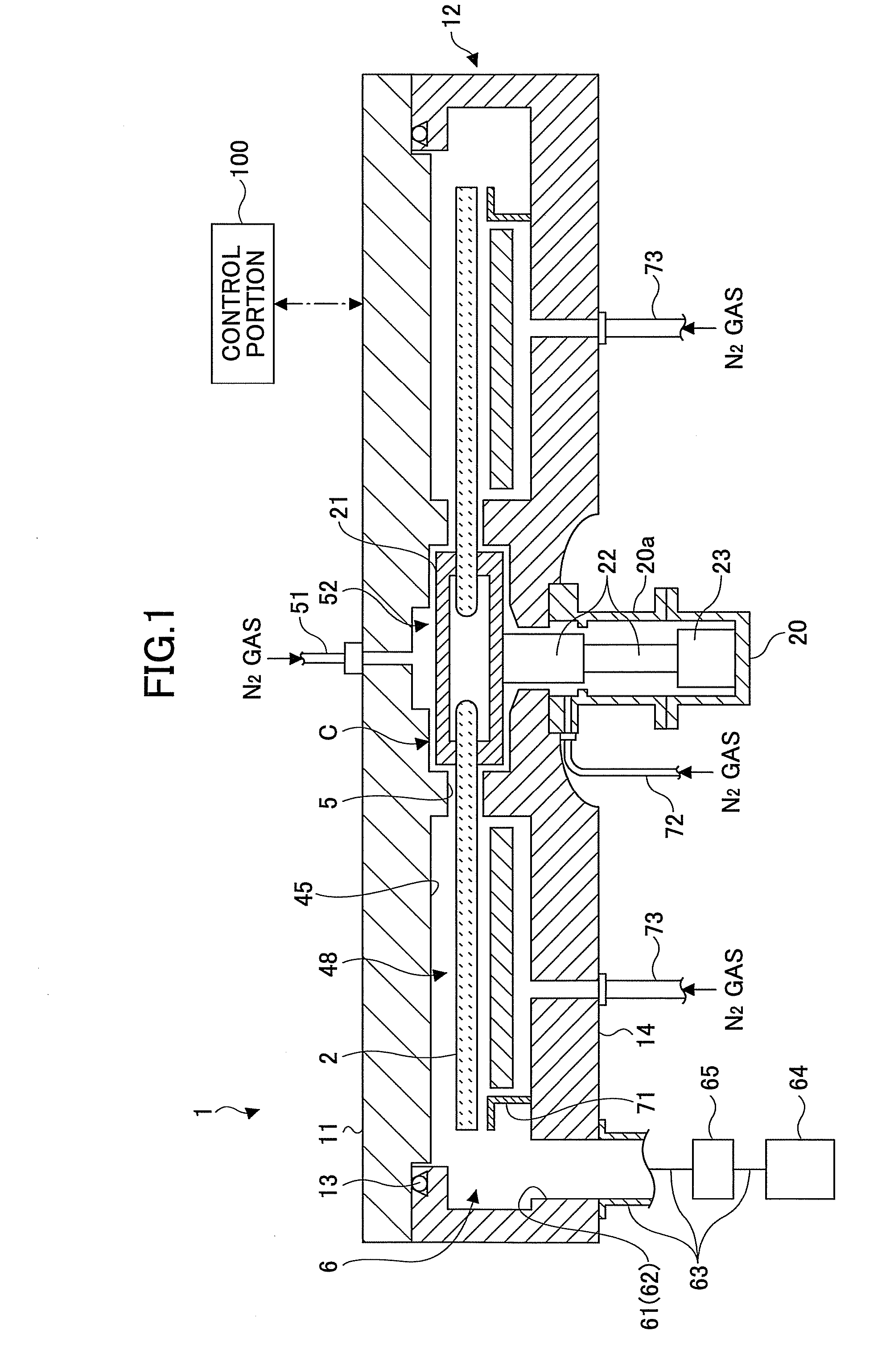
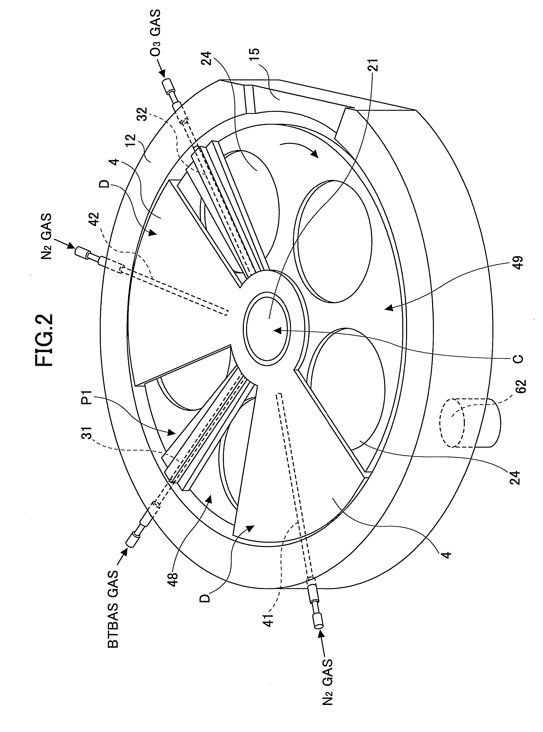
[0087]A film deposition apparatus according to an embodiment of the present invention is provided with ...
PUM
| Property | Measurement | Unit |
|---|---|---|
| pressure | aaaaa | aaaaa |
| diameter | aaaaa | aaaaa |
| height | aaaaa | aaaaa |
Abstract
Description
Claims
Application Information