

Correction of cluster defects in imagers
a cluster defect and imager technology, applied in image enhancement, color signal processing circuits, instruments, etc., can solve the problems of reducing the yield of parts during production, causing severe image quality degradation, and causing the creation of defective pixels
- Summary
- Abstract
- Description
- Claims
- Application Information
AI Technical Summary
Problems solved by technology
Method used
Image

Examples
Embodiment Construction
[0018] In the following detailed description, reference is made to the accompanying drawings, which form a part hereof and show by way of illustration specific embodiments in which the invention may be practiced. These embodiments are described in sufficient detail to enable those skilled in the art to practice the invention, and it is to be understood that other embodiments may be utilized, and that structural, logical, and electrical changes may be made without departing from the spirit and scope of the present invention. The progression of processing steps described is exemplary of embodiments of the invention; however, the sequence of steps is not limited to that set forth herein and may be changed as is known in the art, with the exception of steps necessarily occurring in a certain order.
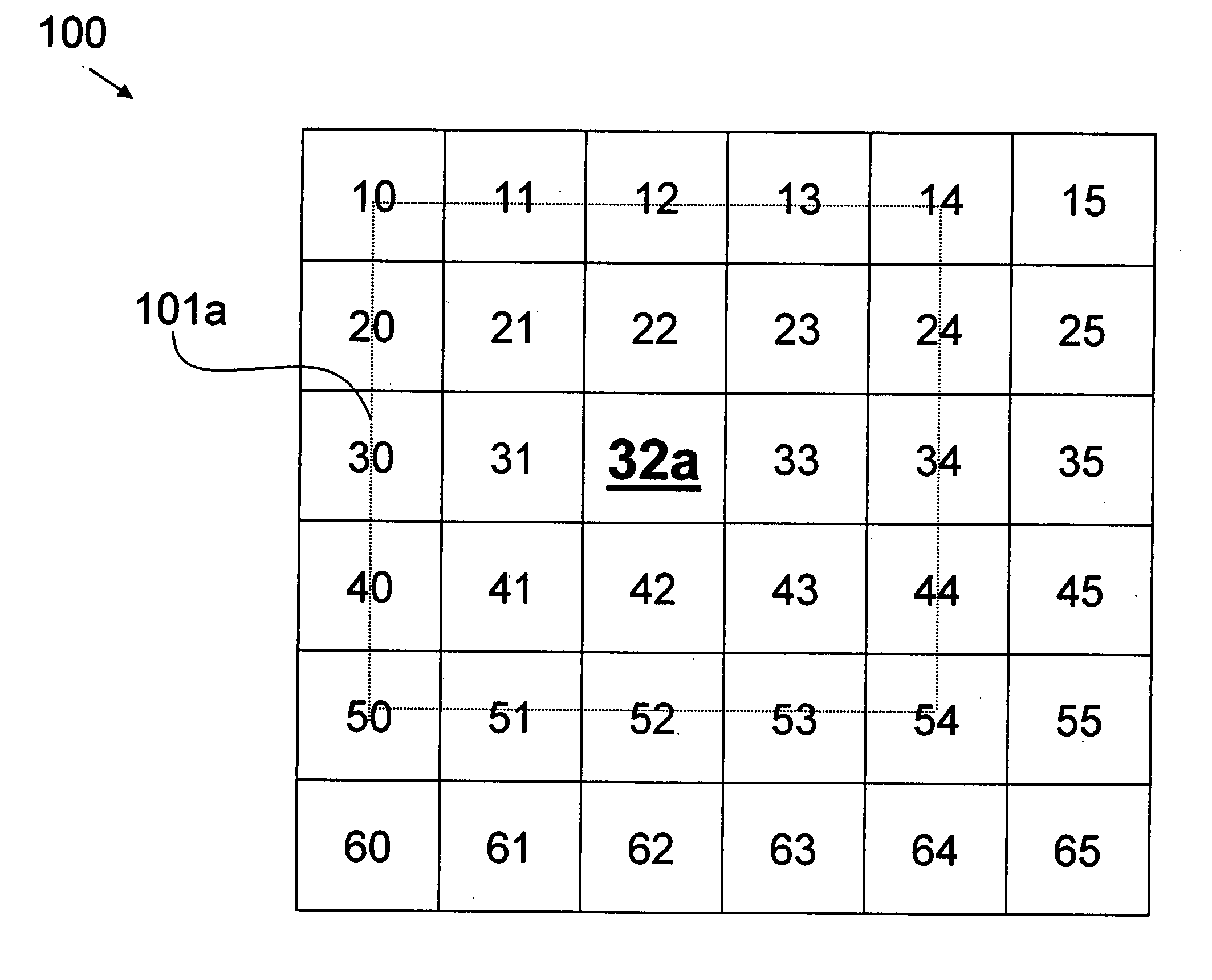
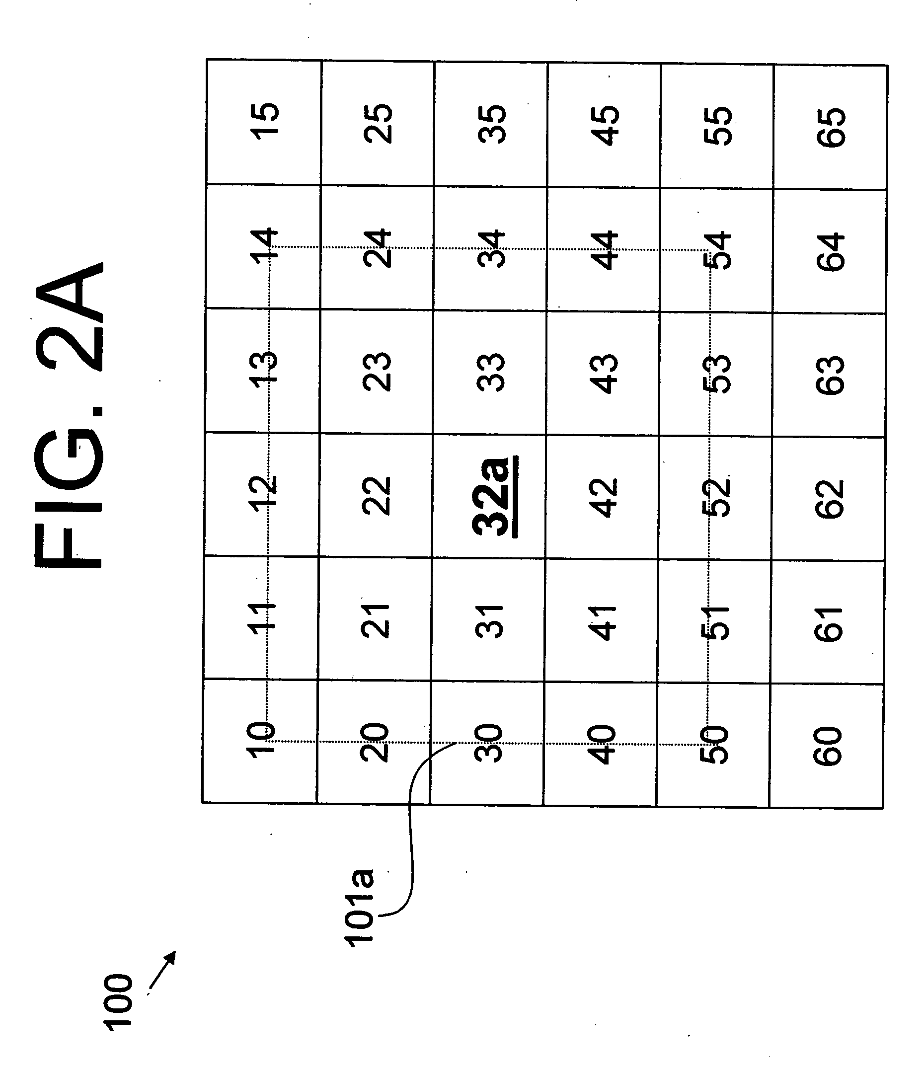
[0019] The term “pixel,” as used herein, refers to a photo-element unit cell containing a photosensor device and associated structures for converting photons to an electrical signal. For purp...
PUM
 Abstract
Description
Claims
Application Information