
Donut-type parallel probe card and method of testing semiconductor wafer using same

Inactive Publication Date: 2007-02-15
SAMSUNG ELECTRONICS CO LTD
View PDF4 Cites 1 Cited by
  • Summary
  • Abstract
  • Description
  • Claims
  • Application Information

AI Technical Summary

Problems solved by technology

However, if the die fails one or more of the tests, the die is either repaired using some form of redundant circuitry within the die, or the die is used with limited functionality, or the die is discarded.
In many cases, die must be discarded, thus lowering the yield and increasing the average cost of semiconductor manufacturing.
The ATE used in the EDS testing is typically very expensive.

Method used


Image

  • Donut-type parallel probe card and method of testing semiconductor wafer using same
  • Donut-type parallel probe card and method of testing semiconductor wafer using same
  • Donut-type parallel probe card and method of testing semiconductor wafer using same

Examples


Embodiment Construction

[0027] Exemplary embodiments of the invention are described below with reference to the corresponding drawings. These embodiments are presented as teaching examples. The actual scope of the invention is defined by the claims that follow.

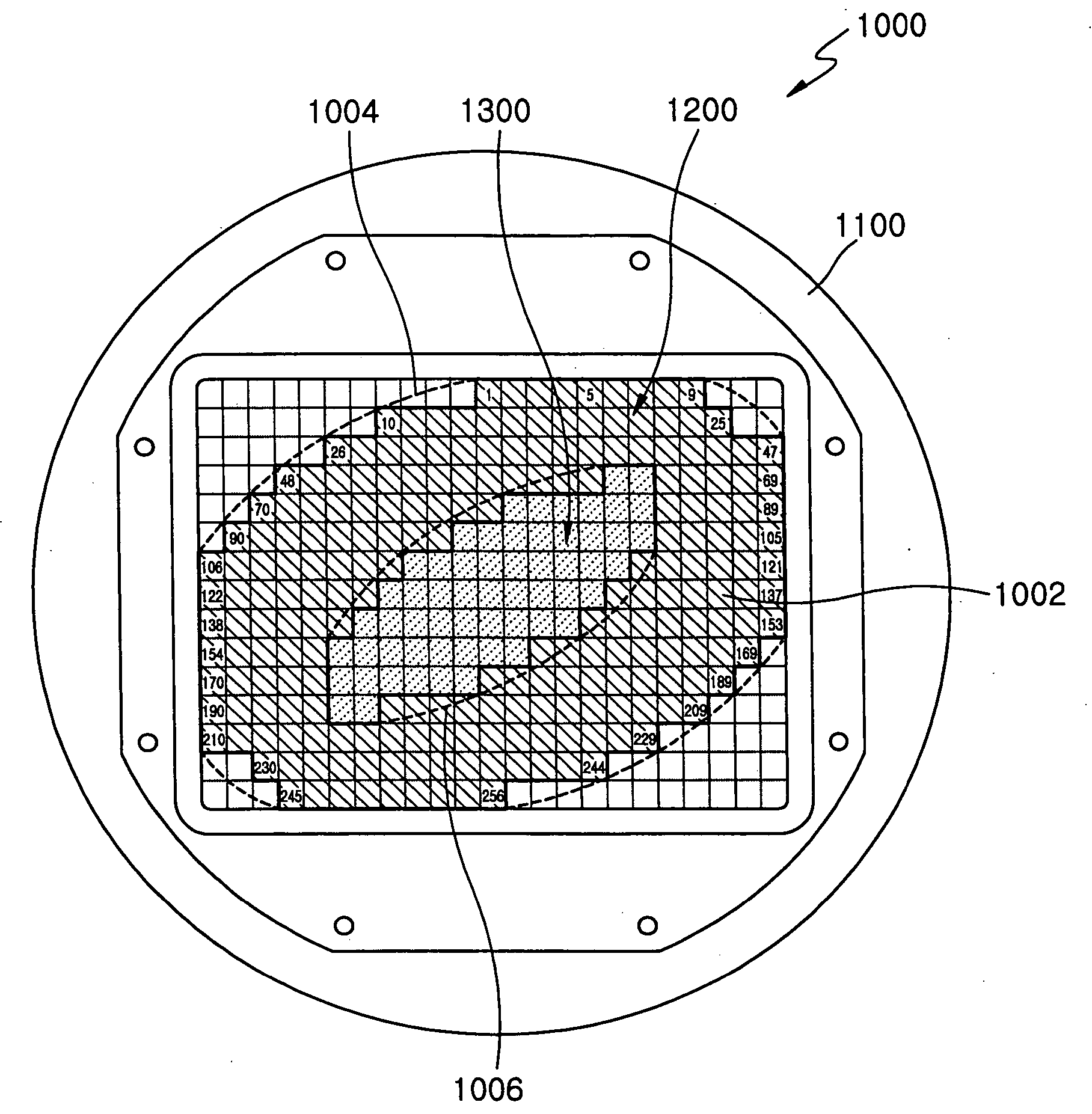
[0028]FIG. 6 is a plan view of a parallel probe card 1000 having a plurality of probing blocks 1002 arranged in a donut shape according to an embodiment of the present invention. The parallel probe card will be referred to hereafter as a donut-type parallel probe card 1000.

[0029] Referring to FIG. 6, donut-type parallel probe card 1000 includes a main substrate 1100 having conductive patterns and probing blocks 1002 installed on a surface of main substrate 1100. Probing blocks 1002 include probes corresponding to pads on respective individual chips. Probing blocks 1002 are described in further detail below with reference to FIG. 9.

[0030] Unlike conventional probing blocks, probing blocks 1002 of donut-type parallel probe card 1000 have a donut sha...


PUM


Abstract

A donut-type parallel probe card comprises a main substrate and a plurality of probing blocks installed on a surface of the main substrate, wherein each probe block comprises a plurality of probes. The probing blocks are arranged to fill a first region having an oval shape and surrounding a second region, and no probing blocks are arranged within the second region.

Description

BACKGROUND OF THE INVENTION [0001] 1. Field of the Invention [0002] Embodiments of the invention relate generally to techniques and equipment for electrically testing a semiconductor wafer. More particularly, embodiments of the invention relate to a parallel probe card used when an electrical die sort (EDS) test and a wafer burn-in test are conducted on a semiconductor wafer. [0003] A claim of priority is made to Korean Patent Application No. 10-2005-0072995 filed on Aug. 9, 2005, the disclosure of which is hereby incorporated by reference in its entirety. [0004] 2. Description of Related Art [0005] Electrical die sort (EDS) testing is commonly used to identify bad die prior to integrated circuit (IC) packaging. In an EDS test, the electrical performance and circuit functioning of each die on a semiconductor wafer is tested. If a die passes all of the tests, the die can be packaged to form a semiconductor device. However, if the die fails one or more of the tests, the die is either ...

Claims


Application Information

Patent Timeline
IPC IPC(8): G01R31/02
CPCG01R1/073H01L22/00
Inventor YOO, SANG-KYUKANG, SUNG-MOCHO, CHANG-HYUN
Owner SAMSUNG ELECTRONICS CO LTD
Features
  • Generate Ideas
  • Intellectual Property
  • Life Sciences
  • Materials
  • Tech Scout
  • Unparalleled Data Quality
  • Higher Quality Content
  • 60% Fewer Hallucinations
Learn More