Liquid crystal display, surface light source device, and information device

a technology of liquid crystal display and surface light source, which is applied in the direction of waveguides, waveguide type devices, instruments, etc., can solve the problems of deteriorating image definition, front surface luminance, and deteriorating image definition, so as to reduce screen glare and the effect of changing the luminance in a minute region

Inactive Publication Date: 2007-02-15
ORMON CORP
View PDF9 Cites 10 Cited by
  • Summary
  • Abstract
  • Description
  • Claims
  • Application Information

AI Technical Summary

Benefits of technology

[0010] In one or more embodiments of the invention, a liquid crystal display where luminance variation in a minute region of a screen is suppressed so that glare on the screen is reduced, and a surface light source device is provided.

Problems solved by technology

In the liquid crystal display described in Japanese Patent Application Laid-Open No. 2002-107706, however, since the light emitted from the liquid crystal panel is diffused, definition of an image is deteriorated and front surface luminance (in this specification, the forward direction of the liquid crystal display is occasionally called the front surface) is deteriorated.
Due to the rough plane formed on the light-emitting plane, however, the definition of an image is deteriorated, and the decrease in the front surface luminance caused by the rough plane cannot be completely recovered by the prism sheet.

Method used


Image

  • Liquid crystal display, surface light source device, and information device
  • Liquid crystal display, surface light source device, and information device
  • Liquid crystal display, surface light source device, and information device

Examples


first embodiment

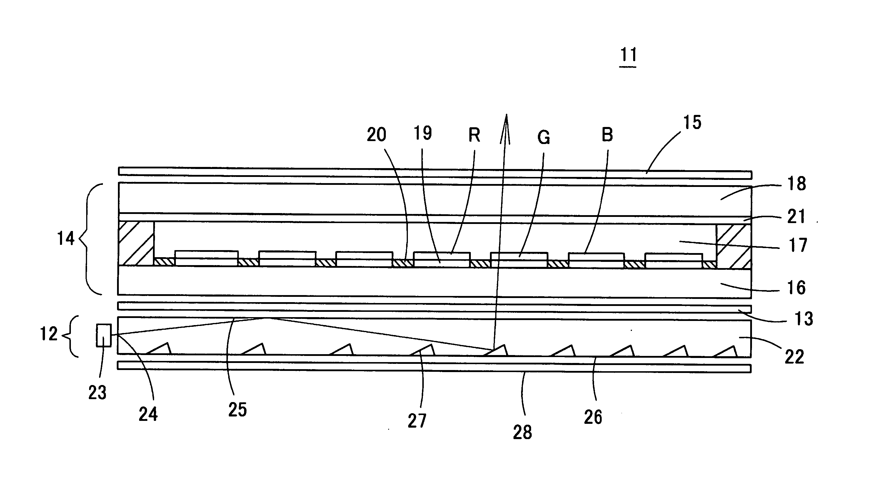
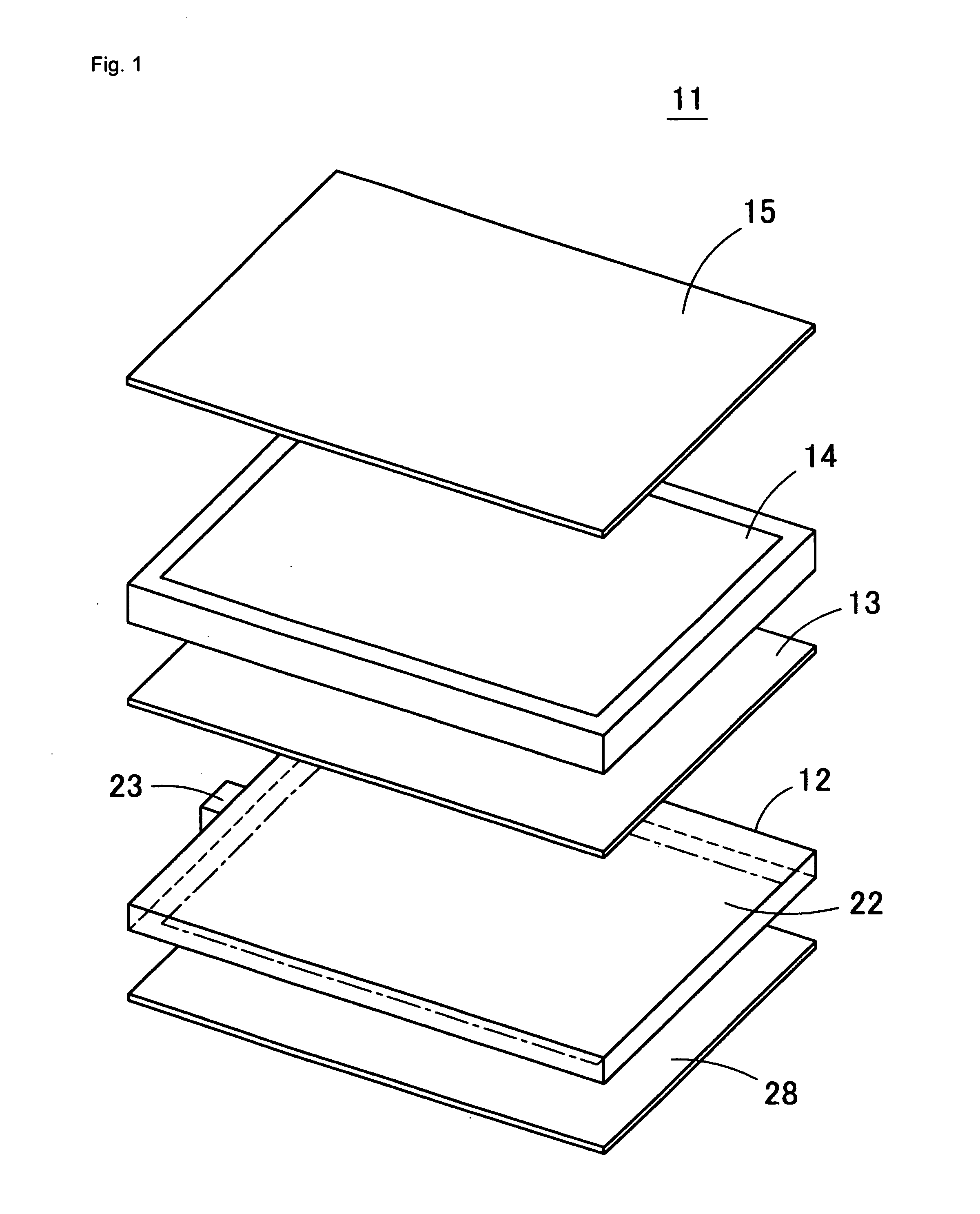
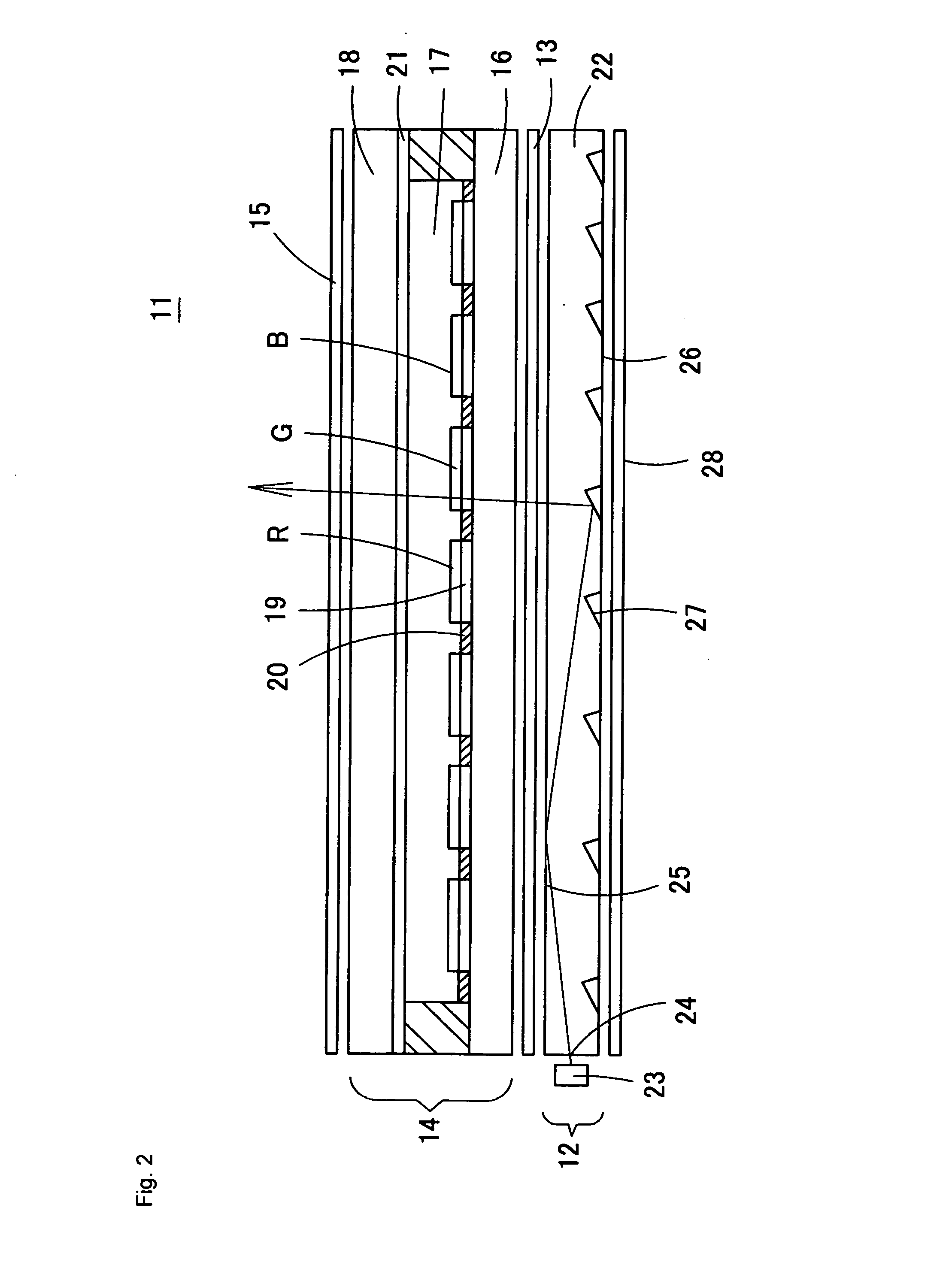
[0058]FIG. 1 shows an exploded perspective view of a liquid crystal display 11 according to the present invention. FIG. 2 shows a schematic sectional view of the liquid crystal display 11. The liquid crystal display 11 is constituted by a surface light source device 12, a liquid crystal panel 14, two polarizing plates 13 and 15, and a light reflecting plate 28. The light reflecting plate 28, the surface light source device 12, the polarizing plate 13, the liquid crystal panel 14 and the polarizing plate 15 are overlapped in this order from a rear face side.

[0059] The liquid crystal panel 14 is not particularly limited, and may have any structure and system. For example, a color liquid crystal panel to be used generally is constituted so that liquid crystal 17 is sealed between two glass substrates 16 and 18 as shown in FIG. 2. Transparent pixel electrodes 19 are formed on an inner surface of the glass substrate 16 on the rear face side, and a red filter R, a green filter G or a blue...

third embodiment

[0115] In the third embodiment, the pattern density of the deflection patterns 27 is small in the vicinity of the light source 23, and the pattern density is larger in positions farther from the light source 23. Concretely, the deflection patterns 27 are arranged as shown in FIGS. 23A and 23B. FIG. 23A shows a diagram illustrating the arrangement of the deflection patterns 27 in the pixels 29 in the vicinity of the light source 23. FIG. 23B shows a diagram illustrating the arrangement of the deflection patterns 27 in the pixels 29 in positions slightly separated from the light source 23. In the vicinity of the light source 23, as shown in FIG. 23A, the number of the deflection patterns 27 in one pixel 29 is reduced, and the pattern area S of one deflection pattern 27 is also reduced. As being farther from the light source 23, as shown in FIG. 23B, for example, the number of the deflection patterns 27 in one pixel 29 is gradually increased, and the pattern area S of one deflection pa...

fourth embodiment

[0119] A fourth embodiment explains a both-surface display type liquid crystal display using the surface light source device 12. In a both surface display type liquid crystal display 41 shown in FIG. 26A, the liquid crystal panel 14 is arranged opposite the light-emitting plane of the light guide plate 22, and a semi-transmissive semi-reflecting film 42 is provided to the front surface of the liquid crystal panel 14. In the liquid crystal display 41, the light emitted from the light-emitting plane of the surface light source device 12 transmits through the liquid crystal panel 14, and the half of the light transmitted through the liquid crystal panel 14 transmits through the semi-transmissive semi-reflecting film 42. An image is recognized on the front surface side of the liquid crystal display 41. The residual half of the light reflected from the semi-transmissive semi-reflecting film 42 transmits through the liquid crystal panel 14 and the light guide plate 22, and an image is rec...


PUM

PropertyMeasurementUnit
hazeaaaaaaaaaa
diameteraaaaaaaaaa
areaaaaaaaaaaa

Abstract

A liquid crystal display has a light guide plate having a light-emitting plane on its one end surface, a light source arranged on a side surface of the light guide plate, and a liquid crystal panel arranged opposite the light-emitting plane of the light guide plate. Deflection patterns are formed on a surface opposite the light-emitting plane of the light guide plate, and the deflection patterns are arranged so that two independent components on the surface opposite the light-emitting plane of the light guide plate are random. In a certain region on the surface opposite the light-emitting plane, when an average value of the number of the deflection patterns included in each region opposite each pixel of the liquid crystal panel is designated by μn and a standard deviation is designated by σn, their ratio satisfies the relationship: 0<σn/μn≦0.154. Light from the light source introduced into the light guide plate is deflected towards the light-emitting plane by the deflection patterns so as to be emitted from the light-emitting plane. The liquid crystal panel is illuminated by the light emitted from the light-emitting plane.

Description

BACKGROUND OF THE RELATED ART [0001] 1. Field of the Invention [0002] The present invention relates to a liquid crystal display in which glare on a display screen is reduced, and a surface light source device. [0003] 2. Description of the Related Art [0004] In liquid crystal displays, when the display screens produce glare, image quality is deteriorated, and thus it is desired that the glare on the screens is reduced. Techniques for suppressing the glare on the screens in the liquid crystal displays have been proposed for example, in Japanese Patent Application Laid-Open Nos. 2002-107706 and 11-352312 (1999). [0005] In a liquid crystal display described in Japanese Patent Application Laid-Open No. 2002-107706, the following method is proposed. According to this method, a diffusion layer and a glare-proof layer, provided on a front surface of a liquid crystal panel, diffuses light emitted from the liquid crystal panel, and the total haze value is set to 30 to 80%, so that the glare o...

Claims


Application Information

Patent Timeline
Patent Type & Authority Applications(United States)
IPC IPC(8): G02F1/1335
CPCG02B6/0036G02F1/133615G02B6/0061G02B6/0038Y10S385/901
Inventor WATANUKI, KENKURATA, GOUOSAKURAI, KENJIFUNAMOTO, AKIHIROAOYAMA, SHIGERU
Owner ORMON CORP
Why Eureka
Try Eureka