Display device and electronic apparatus having the display device

a display device and electronic equipment technology, applied in static indicating devices, instruments, optics, etc., can solve the problems of interrupting the downsizing of a display panel, increasing etc., and achieve the effect of reducing the luminance, and reducing the size of the monitoring elemen

Inactive Publication Date: 2007-08-23
SEMICON ENERGY LAB CO LTD
View PDF22 Cites 8 Cited by
  • Summary
  • Abstract
  • Description
  • Claims
  • Application Information

AI Technical Summary

Benefits of technology

[0009] In view of the foregoing problems, it is an object of the present invention to provide a display device in which an influence of variations in current value of a light-emitting element, which are caused by an environmental temperature change and a change with time, can be suppressed and which can be designed without upsizing a monitoring element when a pixel size of a display portion is increased.
[0018] By using a display device according to the present invention, variations in luminance due to variations in current value of a light-emitting element, which are caused by an environmental temperature change and a change with time, can be suppressed. Further, in the display device according to the present invention, since it is not necessary to provide a monitoring element into the same size as that of a pixel in a display portion, the monitoring element can be downsized. In addition, by downsizing the monitoring element, downsizing of a display device, in other words, a narrow frame of the display device can be achieved.

Problems solved by technology

However, as a pixel size of the display portion increases, the size of the monitoring element is also necessary to be increased; therefore, there is a problem of interrupting downsizing of a display panel.

Method used


Image

  • Display device and electronic apparatus having the display device
  • Display device and electronic apparatus having the display device
  • Display device and electronic apparatus having the display device

Examples


embodiment mode 1

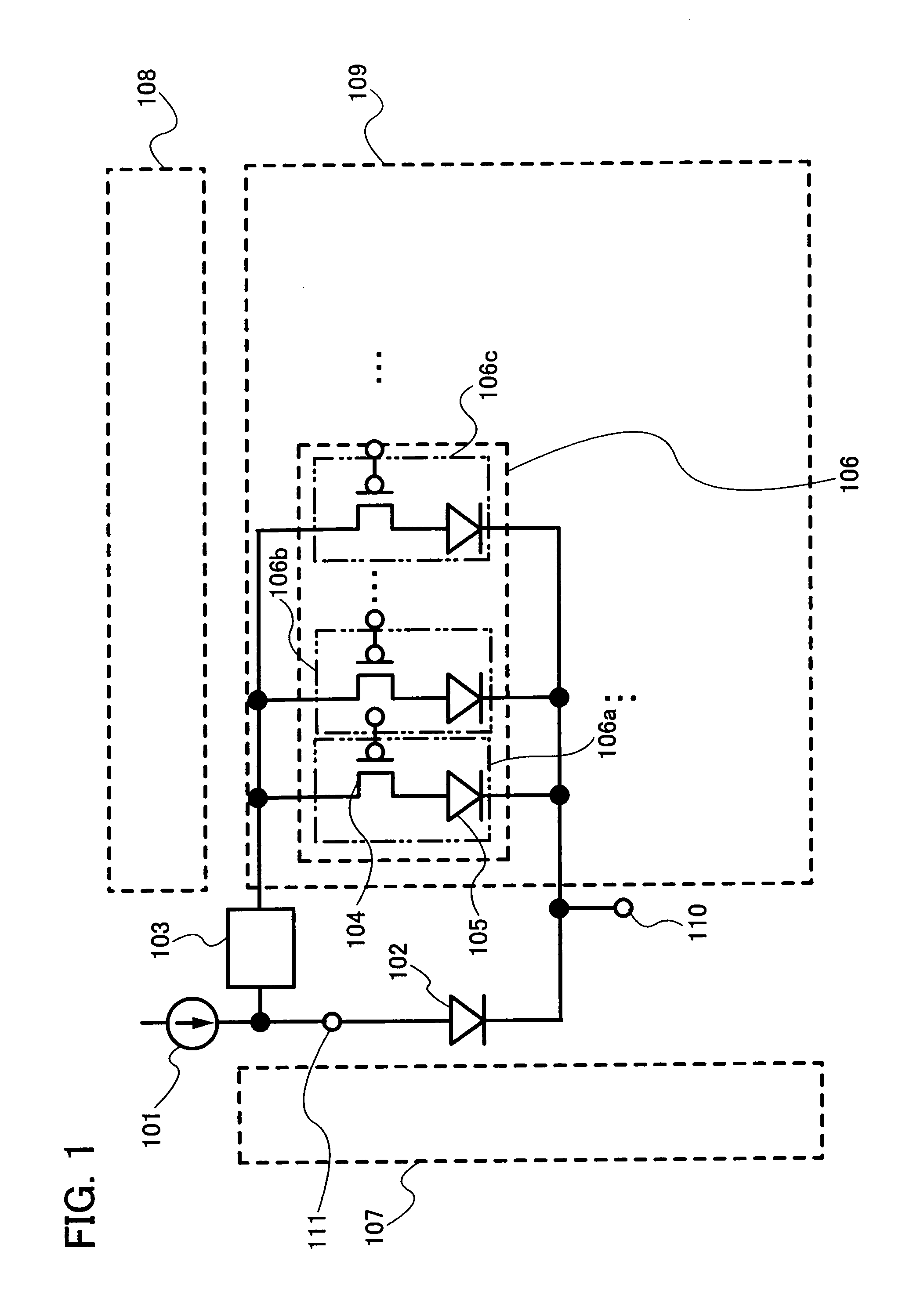
[0053] This embodiment mode will describe a basic principle of temperature and deterioration compensation in a display device according to the present invention. FIG. 1 shows a schematic diagram of a display device which has a temperature and deterioration compensation circuit.

[0054] A display device according to the present invention includes a gate driver 107, a source driver 108, and a pixel portion 109. The pixel portion 109 includes a plurality of pixels 106. In the pixel portion 109, the pixel 106 includes a plurality of sub-pixels 106a, 106b, and 106c. It is to be noted that each of the plurality of sub-pixels is provided with a driving transistor (driving TFT) 104 and a light-emitting element 105. In FIG. 1, the plurality of sub-pixels are formed of three sub-pixels 106a, 106b, and 106c, but the present invention is not limited thereto, and two or more sub-pixels may be provided in one pixel.

[0055] In this specification, a pixel includes a color element forming one image a...

embodiment mode 2

[0075] This embodiment mode will describe a configuration which is different from that of the display device described in the above embodiment mode. In this embodiment mode, a configuration in which precision of deterioration compensation is further enhanced will be described.

[0076] When a display device is continuously used for a long time, a discrepancy is generated in deterioration progression between a monitoring element and a light-emitting element. As the display device is used longer, the discrepancy grows bigger, leading a lowered function of compensating deterioration.

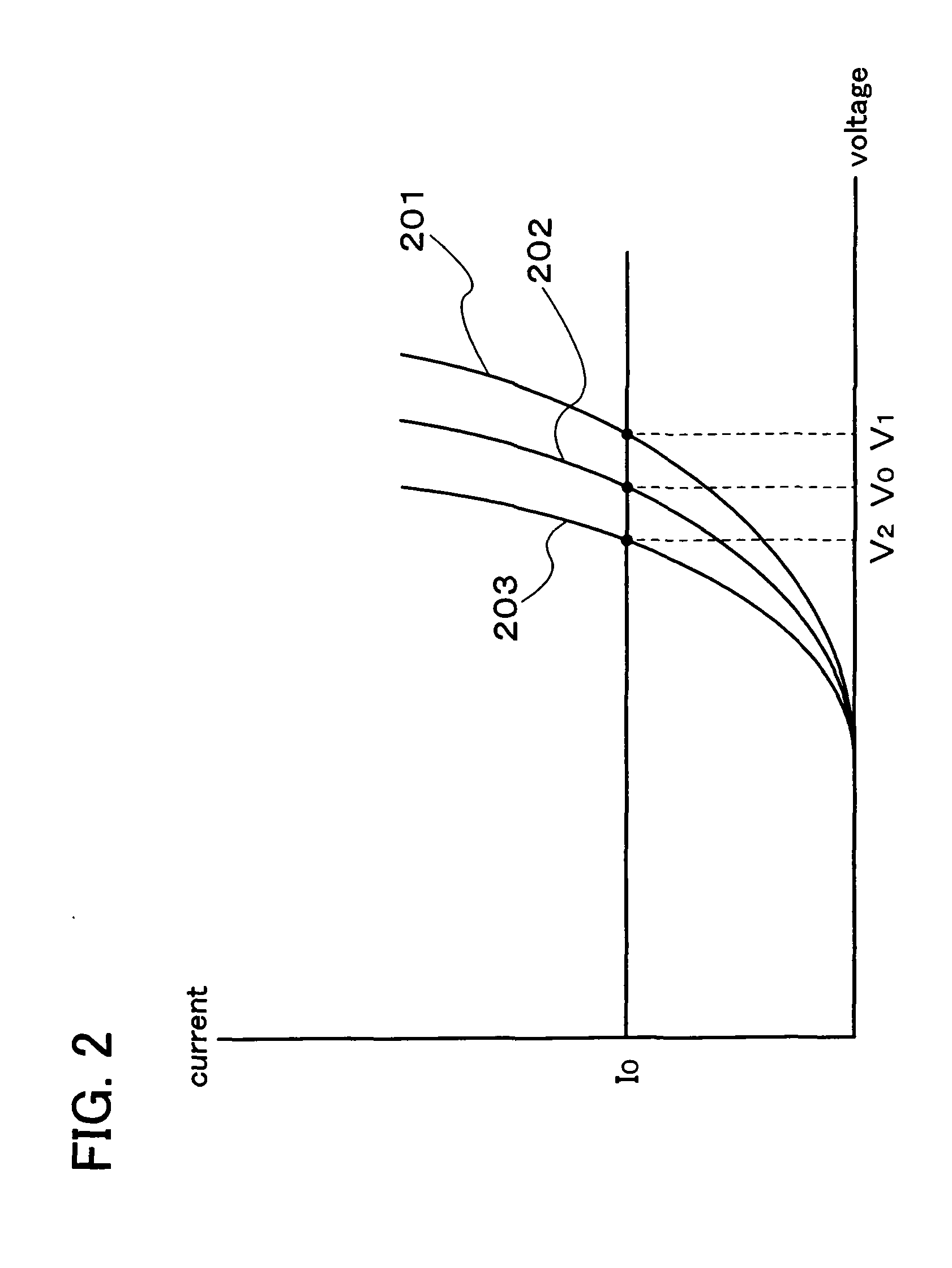
[0077] Here, description is made on a case where a discrepancy is generated in deterioration progression with reference to FIG. 4. Initial characteristics of voltage-current (VI) characteristics of the monitoring element 102 and the light-emitting element 105 are denoted by a line 401, VI characteristics after deterioration of the monitoring element 102 in a case where the display device is used for a certai...

embodiment mode 3

[0092] This embodiment mode will describe a configuration which is different from that of the display device described in the above embodiment modes. In this embodiment mode, a configuration of a display device, in which precision of deterioration compensation is improved while maintaining precision of temperature compensation, will be described with reference to FIG. 6.

[0093] A display device includes a current source 601, monitoring elements 602a and 602b, a voltage follower circuit 603, switches 606a and 606b, and a pixel 610. The pixel 610 includes a plurality of sub-pixels 610a, 610b, and 610c, and each sub-pixel includes a driving transistor 604 and a light-emitting element 605. In FIG. 6, the plurality of sub-pixels is formed of three sub-pixels 610a, 610b, and 610c, but the present invention is not limited thereto and two or more sub-pixels may be provided in one pixel. In addition, similarly to Embodiment Mode 1, in a case where the light-emitting element is formed of an E...


PUM


Abstract

A light-emitting element has a property that a resistance value (internal resistance) changes in accordance with an environmental temperature. It is an object to downsize a monitoring element which corrects an influence of variations in current value of the light-emitting element, which are caused by an environmental temperature change and a change with time. A pixel includes a plurality of sub-pixels, areas of light-emitting elements provided in the individual sub-pixels are made to be different from each other, and an area of a monitoring element is made to be the same as an area of the light-emitting element in any of the sub-pixels, thereby correcting light-emission of the pixel by the monitoring element.

Description

BACKGROUND OF THE INVENTION [0001] 1. Field of the Invention [0002] The present invention relates to a display device, in particular, a display device including light-emitting elements arranged in active-matrix. In addition, the present invention relates to an electronic apparatus provided with the display device. [0003] 2. Description of the Related Art [0004] In recent years, demands for thin displays mainly applied to TVs, PC monitors, mobile terminals, and the like have rapidly increased and further development has been promoted. The thin displays include a liquid crystal display device (LCD) and a display device equipped with a light-emitting element. In particular, an active matrix display using a light-emitting element is expected as a next-generation display for its features of high response speed, wide viewing angle, and the like in addition to advantages of a conventional LCD, such as thinness, lightness in weight, and high image quality and has been partially put in pract...

Claims


Application Information

Patent Timeline
Patent Type & Authority Applications(United States)
IPC IPC(8): H01L29/76H05B44/00
CPCG02F1/0123G02F2001/134345G02F2201/58H01L27/3269G09G2320/029G09G2320/041G09G2320/043G09G3/3275G02F1/134345H10K59/13
Inventor YAMAZAKI, SHUNPEIOSAME, MITSUAKIIWABUCHI, TOMOYUKITAKAHASHI, KEINOZAWA, RYOSATO, MIZUKIFUKUMOTO, RYOTA
Owner SEMICON ENERGY LAB CO LTD
Why Eureka
Try Eureka