

Light Emitting Device
- Summary
- Abstract
- Description
- Claims
- Application Information
AI Technical Summary
Benefits of technology
Problems solved by technology
Method used
Image

Examples
embodiment mode 1
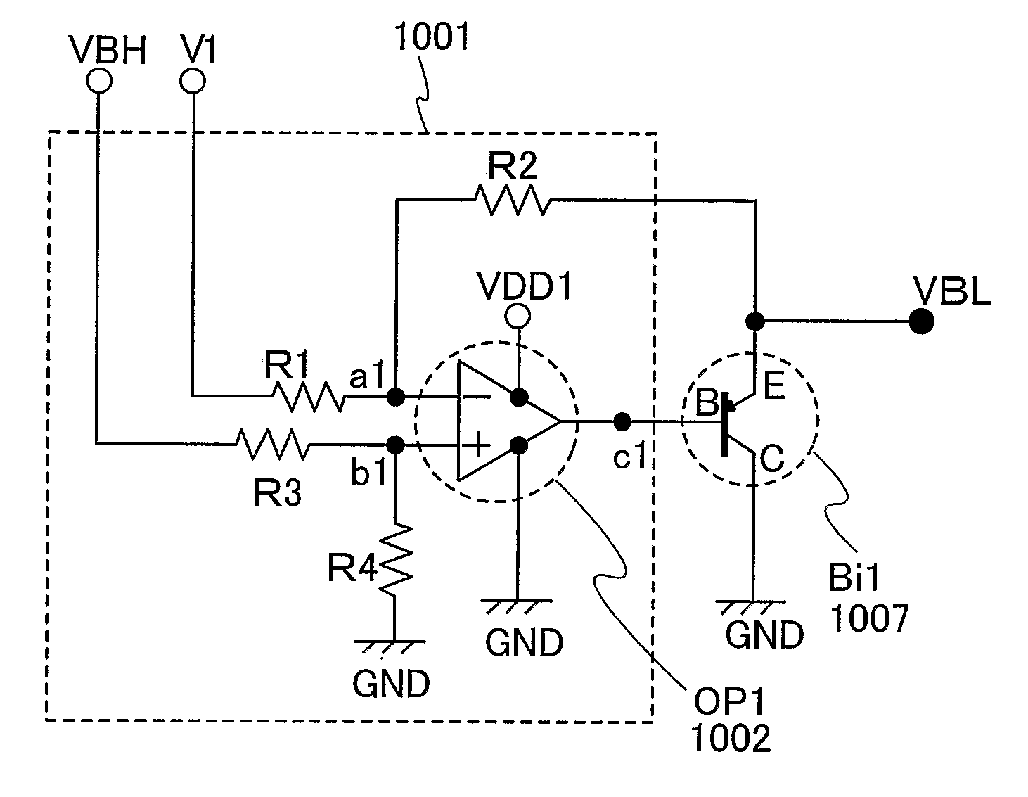
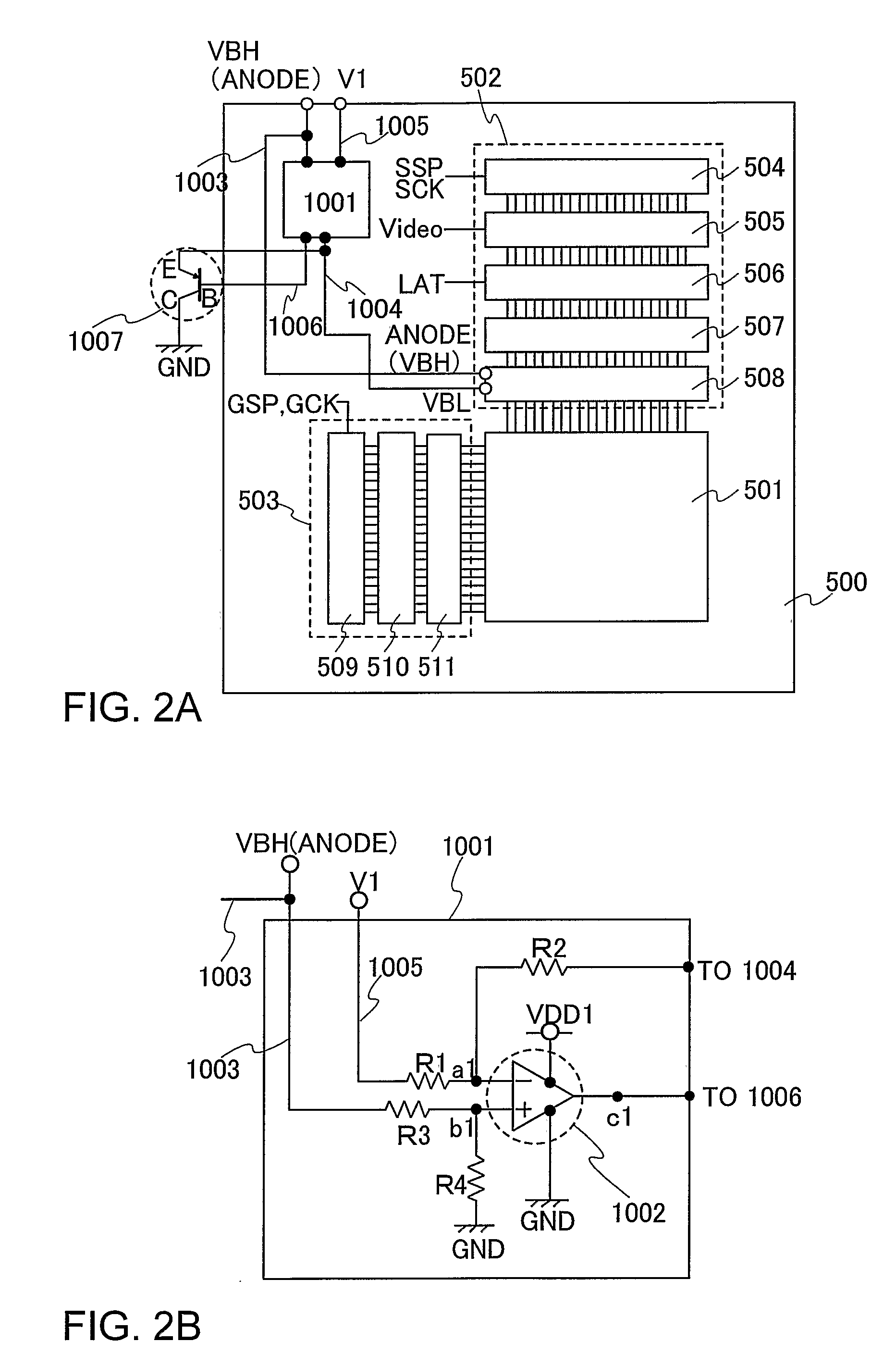
[0051]This embodiment mode is described with reference to FIGS. 1, 2A, and 2B.
[0052]FIG. 1 is a circuit diagram of a potential generating circuit of this embodiment mode. As shown in FIG. 1, the potential generating circuit includes resistors R1 to R4, an operational amplifier (OP1) 1002, and a bipolar transistor (Bi1) 1007.
[0053]Two power source connecting terminals of the operational amplifier OP1 are inputted with a high power potential (VDD1) and a low power potential (GND) respectively. Further, an output terminal c1 of the operational amplifier (OP1) is connected to a base terminal B of the bipolar transistor (Bi1). The base terminal B of the bipolar transistor (Bi1) is connected to the output terminal c1 of the operational amplifier (OP1) and a collector terminal C thereof is connected to the low power potential (GND).
[0054]The resistor R1 has one terminal connected to a high power potential (V1) and the other terminal connected to an input terminal al of the operational ampl...
embodiment mode 2
[0070]FIG. 3 is a circuit diagram of a potential generating circuit of this embodiment mode. As shown in FIG. 3, the potential generating circuit includes the resistors R1 to R4 and the operational amplifier (OP1).
[0071]Two power source connecting terminals of the operational amplifier (OP1) are inputted with the high power potential (VDD1) and the low power potential (GND) respectively.
[0072]The resistor R1 has one terminal connected to the high power potential (V1) and the other terminal connected to an input terminal al of an operational amplifier (OP1) 1102. The resistor R2 has one terminal connected to the input terminal a1 of the operational amplifier (OP1) 1102 and the other terminal connected to an output terminal cl of the operational amplifier (OP1) 1102. The resistor R3 has one terminal connected to a high power potential (VBH) and the other terminal connected to an input terminal b1 of the operational amplifier (OP1) 1102. The resistor R4 has one terminal connected to th...
embodiment mode 3
[0085]As described in Embodiment Modes 1 and 2, the invention is preferably applied to an electronic device which is required to have a high resolution display portion as the invention can suppress power consumption of an EL display device and variations in luminance of the display portion caused by the high resolution of the pixels. Examples are a television device (a television, a television receiver), a camera such as a digital camera, and a digital video camera, a portable phone device (a portable phone), a portable information terminal such as a PDA, a portable game machine, a monitor, a computer, an audio reproducing device such as a car audio set, and an image reproducing device provided with a recording medium such as a home game machine. Specific examples of these are described with reference to FIGS. 11A to 11F.
[0086]For example, the invention can be applied to a portable information terminal shown in FIG. 11A, a digital video camera shown in FIG. 11B, a portable phone sho...
PUM
 Abstract
Description
Claims
Application Information