Light-emitting device

a technology of light-emitting devices and electroluminescent layers, which is applied in the direction of static indicating devices, solid-state devices, instruments, etc., can solve the problems of sputtering damage to the electroluminescent layer, and suppress the luminance variation among pixels caused by the threshold voltage variation of driving transistors, so as to reduce the luminance of light-emitting elements caused by deterioration of electroluminescent layers.

Active Publication Date: 2015-05-12
SEMICON ENERGY LAB CO LTD
View PDF223 Cites 7 Cited by
  • Summary
  • Abstract
  • Description
  • Claims
  • Application Information

AI Technical Summary

Benefits of technology

[0008]In general, a surface of a conductive film which is used as an anode of a light-emitting element is less likely to be oxidized in the air than that of a conductive film which is used as a cathode of a light-emitting element. In addition, because a conductive film which is used as an anode of a light-emitting element is generally formed by a sputtering method, when the anode is formed over an electroluminescent layer containing an electroluminescent material, the electroluminescent layer tends to be damaged by sputtering. In view of the above, a light-emitting element in which an anode, an electroluminescent layer, and a cathode are stacked in this order can be manufactured through an easy process and can easily achieve high emission efficiency. However, when an n-channel driving transistor is used in combination with the above light-emitting element, a source of the driving transistor is connected to the anode of the light-emitting element. In that case, when the voltage between the anode and the cathode of the light-emitting element is increased owing to deterioration of an electroluminescent material, the potential of the source of the driving transistor is increased, whereby the voltage between a gate and the source (gate voltage) of the driving transistor is decreased. Accordingly, drain current of the driving transistor, that is, current supplied to the light-emitting element is decreased, resulting in a decrease in luminance of the light-emitting element.
[0009]In view of the above problem, an object of one embodiment of the present invention is to provide a light-emitting device in which variation in luminance among pixels caused by variation in threshold voltage of driving transistors can be suppressed. Another object of one embodiment of the present invention is to provide a light-emitting device in which a decrease in luminance of a light-emitting element caused by deterioration of an electroluminescent layer can be suppressed.
[0015]With the above structure, in one embodiment of the present invention, variation in luminance among pixels caused by variation in threshold voltage of driving transistors can be suppressed. Further, in one embodiment of the present invention, a decrease in luminance of a light-emitting element caused by deterioration of an electroluminescent layer can be suppressed.

Problems solved by technology

In addition, because a conductive film which is used as an anode of a light-emitting element is generally formed by a sputtering method, when the anode is formed over an electroluminescent layer containing an electroluminescent material, the electroluminescent layer tends to be damaged by sputtering.

Method used


Image

  • Light-emitting device
  • Light-emitting device
  • Light-emitting device

Examples


embodiment 1

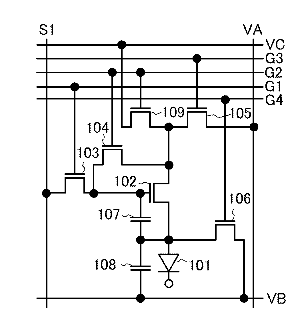
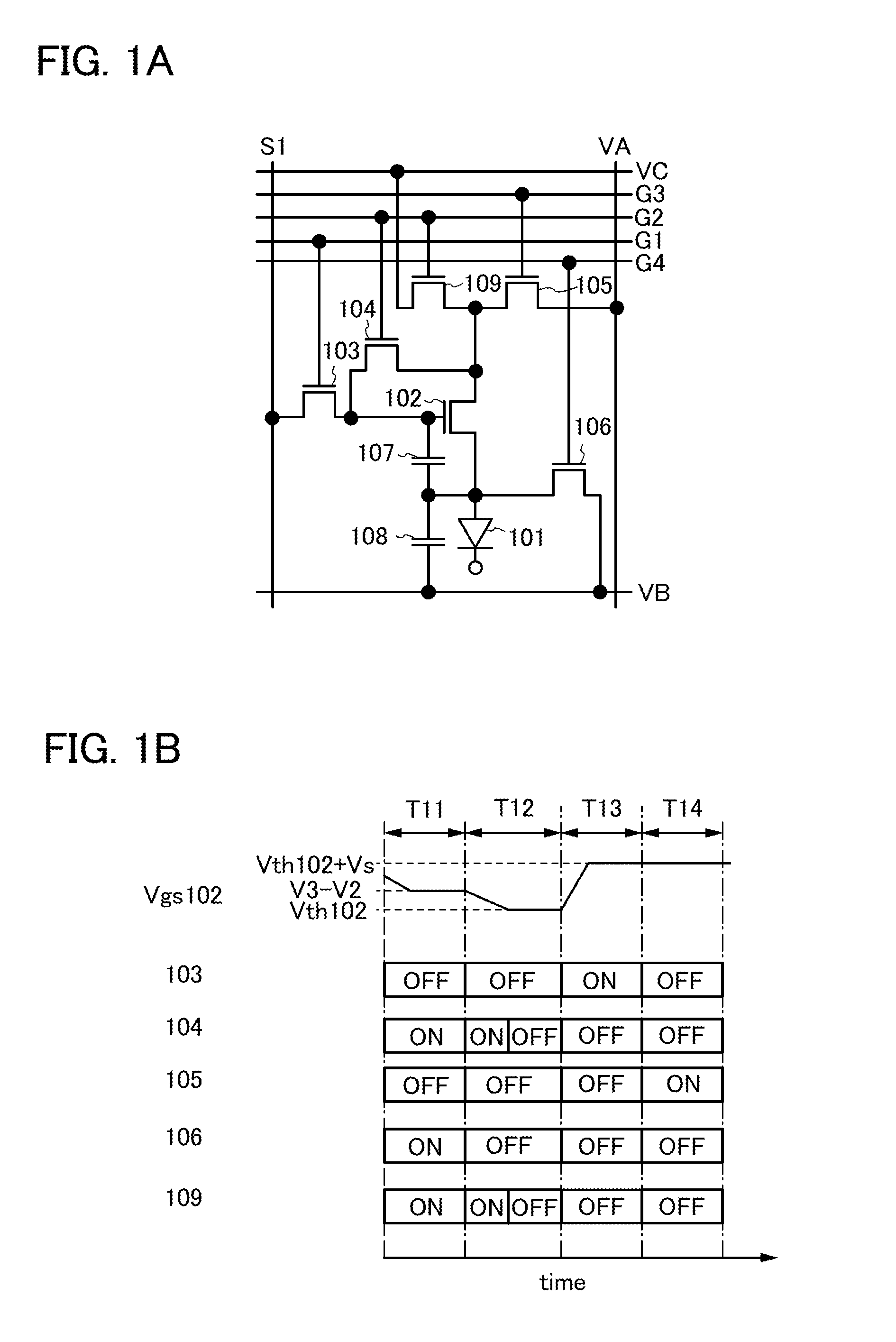
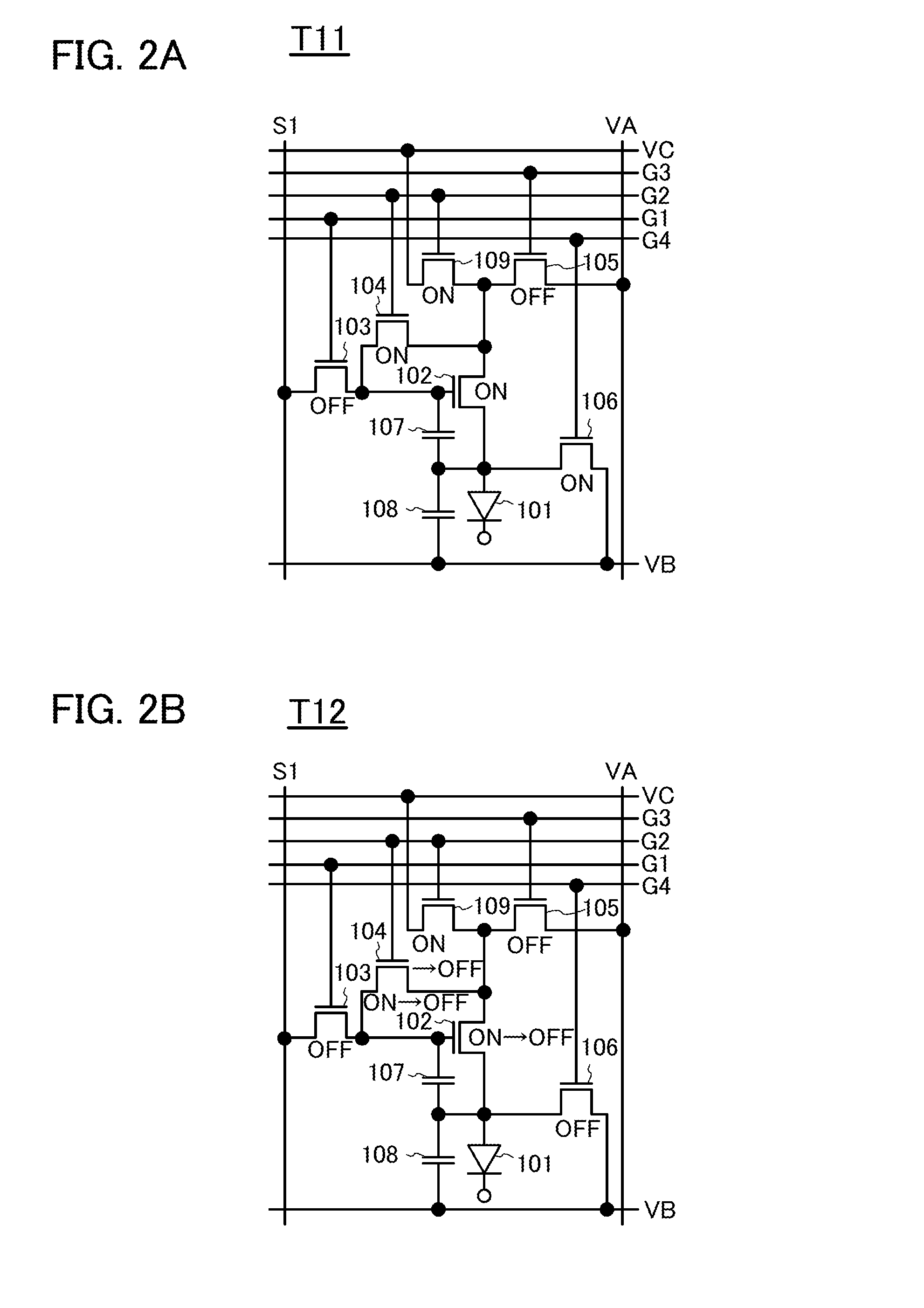
[0048]A light-emitting device in this embodiment includes a pixel portion. An example of the pixel portion in the light-emitting device in this embodiment will be described with reference to FIGS. 1A and 1B.

[0049]As illustrated in FIG. 1A, the pixel portion includes a signal line S1, a power supply line VA, a power supply line VB, a power supply line VC, a scan line G1, a scan line G2, a scan line G3, a scan line G4, a light-emitting element 101, a transistor 102, a transistor 103, a transistor 104, a transistor 105, a transistor 106, a capacitor 107, a capacitor 108, and a transistor 109.

[0050]In the light-emitting device in FIG. 1A, the transistors are field-effect transistors. A source and a drain of each transistor are interchanged in some cases depending on a structure or operation conditions of the transistor.

[0051]For example, one pixel may be constituted by one pixel circuit including the light-emitting element 101, the transistor 102, the transistor 103, the transistor 104,...

embodiment 2

[0088]In this embodiment, a specific structure of a pixel of a light-emitting device according to one embodiment of the present invention will be described.

[0089]FIG. 5 illustrates an example of a top view of the pixel illustrated in FIG. 1A. Note that in the top view of the pixel in FIG. 5, various insulating films are omitted in order to clearly show the layout of the pixel. Further, in the top view of the pixel in FIG. 5, the anode, the electroluminescent layer, and the cathode are omitted in order to clearly show the layout of the transistors and the capacitors included in the pixel.

[0090]FIG. 6 is a cross-sectional view taken along dashed lines A1-A2 and A3-A4 in the top view in FIG. 5.

[0091]The transistor 103 includes, over a substrate 800 having an insulating surface, a conductive film 801 functioning as a gate, a gate insulating film 802 over the conductive film 801, a semiconductor layer 803 positioned over the gate insulating film 802 to overlap with the conductive film 80...

embodiment 3

[0211]In this embodiment, an example of a specific structure of a light-emitting device according to one embodiment of the present invention will be described. In FIG. 11, a block diagram of a light-emitting device in this embodiment is shown as an example. Note that in the block diagram in FIG. 11, circuits in the light-emitting device are classified according to their functions and are illustrated as separated blocks. However, it is difficult to classify actual circuits according to their functions completely and one circuit may have a plurality of functions.

[0212]The light-emitting device shown in FIG. 11 includes a pixel portion 500 including a plurality of pixels, a scan line driver circuit 510 which selects pixels per line, and a signal line driver circuit 520 which controls an input of an image signal to the pixels in the selected line.

[0213]The structure of the pixel portion 500 can be, for example, the structure of the pixel portion in the light-emitting device described in...


PUM


Abstract

A light-emitting device according to one embodiment of the present invention includes a light-emitting element, a first transistor whose source is electrically connected to an anode of the light-emitting element, a second transistor which controls whether an image signal is input to a gate of the first transistor, a third transistor which controls electrical connection and disconnection between the gate and a drain of the first transistor, a fourth transistor which controls whether a first power supply potential is supplied to the drain of the first transistor, a fifth transistor which controls whether a second power supply potential is supplied to the anode of the light-emitting element, a first capacitor which holds a voltage between the gate and the source of the first transistor, and a second capacitor electrically connected in series with the first capacitor and electrically connected in series with the light-emitting element.

Description

BACKGROUND OF THE INVENTION[0001]1. Field of the Invention[0002]The present invention relates to a light-emitting device in which a transistor is provided in each pixel.[0003]2. Description of the Related Art[0004]Because display devices using light-emitting elements have high visibility, is suitable for reduction in thickness, and do not have limitations on viewing angles, they have attracted attention as an alternative to CRTs (cathode ray tubes) or liquid crystal display devices. Specific structures of active matrix display devices using light-emitting elements differ depending on manufacturers. In general, at least a light-emitting element, a transistor (switching transistor) which controls input of a video signal to a pixel, and a transistor (driving transistor) which controls the amount of current supplied to the light-emitting element are provided in each pixel.[0005]When all the transistors in the pixels have the same polarity, it is possible to omit some of steps for manufa...

Claims


Application Information

Patent Timeline
Patent Type & Authority Patents(United States)
IPC IPC(8): G09G3/30H01L27/32H01L51/52G09G3/10H01L51/50H01L27/12
CPCG09G2300/0861G09G2300/0852H01L27/3262H01L51/5218H01L51/5265G09G2320/045H01L27/3206H01L27/322H01L27/1225H01L27/1255H01L51/506H10K59/30H10K59/38H10K59/1213H10K50/155H10K59/876H10K59/80518G09G3/30G09G2320/0233G09G2300/043G09G2300/0842G09G2320/043H10K50/818H10K50/852
Inventor KOYAMA, JUN
Owner SEMICON ENERGY LAB CO LTD
Why Eureka
Try Eureka