MEMS package and method of forming the same

a technology of mems and packaging, applied in the field of wafer level packaging methods for microelectromechanical systems, can solve the problems of high cost and prohibitive cost of large-scale adoption of mems devices, and the cost of pre-formed cavity-type packaging in which three components are required to form the package (the die, the lid) is high

Inactive Publication Date: 2007-03-01
FREESCALE SEMICON INC
View PDF17 Cites 17 Cited by
  • Summary
  • Abstract
  • Description
  • Claims
  • Application Information

AI Technical Summary

Problems solved by technology

MEMS packaging continues to represent the largest and most prohibitive cost associated with large scale adoption of MEMS devices.
However, this pre-formed cavity-type packaging in which three components are required to form the package (the die, the cavity structure and the lid) is expensive because the actual package lid attachment requires precise processing to prevent contamination of the enclosed MEMS die.
These types of cavity packages are also relatively expensive and performed at the single device level.

Method used


Image

  • MEMS package and method of forming the same
  • MEMS package and method of forming the same
  • MEMS package and method of forming the same

Examples


Embodiment Construction

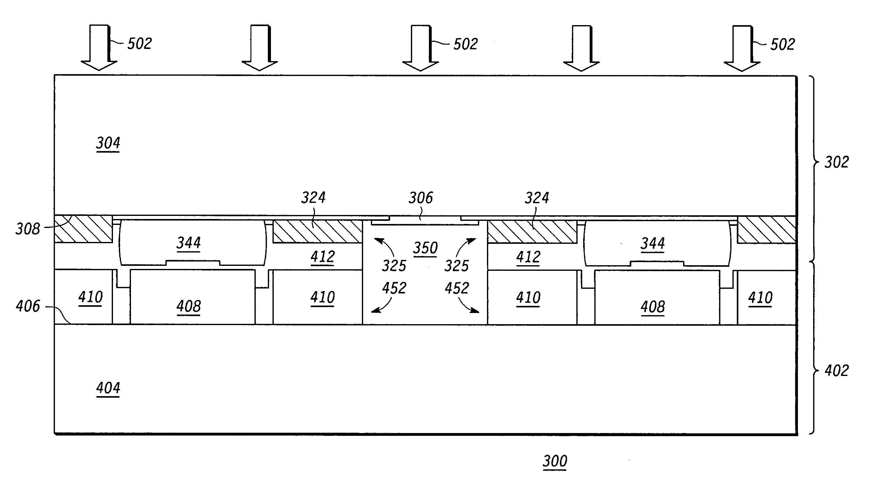
[0010] The following detailed description of the invention is merely exemplary in nature and is not intended to limit the invention or the application and uses of the invention. Furthermore, there is no intention to be bound by any theory presented in the preceding background of the invention or the following detailed description of the invention. Provided is a MEMS device package and a method of fabricating the MEMS device package that incorporates the substrate upon which the MEMS device is formed as a defining part of the package thus requiring fewer manufacturing step to form the package. The package is formed at the wafer level prior to singulation of the MEMS device wafer into individual MEMS die.

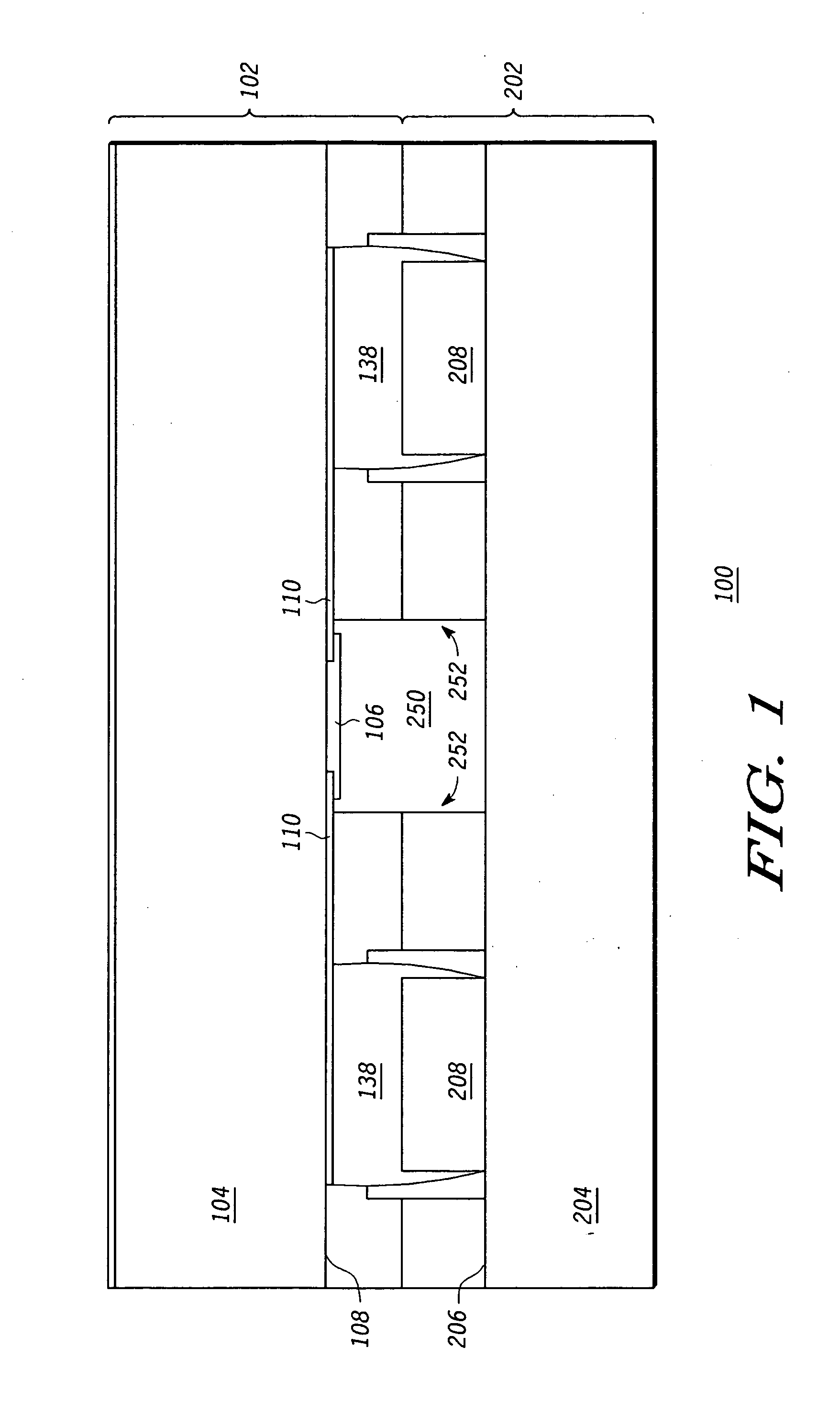
[0011]FIG. 1 is a cross-sectional view of a MEMS package 100 that may be manufactured according to an exemplary process of the present invention. MEMS package 100 is formed by bonding a first component 102 and a second component 202 that when coupled to said first component 102 forms...


PUM


Abstract

A MEMS package (100, 300) and method of fabrication include a package (100, 300) that is formed by bonding a first component (102, 302), which includes a MEMS device (106, 306) and a substrate (104, 304) upon which the MEMS device (106, 306) was formed as a part thereof, to a second component (202, 402) during wafer level packaging. The first component (102, 302) is bonded to the second component (202, 402) using bump bonding or coined wire bonding. The MEMS device (106, 306) resides in a sealed cavity (250, 350) defined by a collar structure (252, 352) formed by the two components (101, 202, 302, 402). The collar structure (252, 352) provides a sealed airspace in which the MEMS device (106, 306) resides and operates.

Description

FIELD OF THE INVENTION [0001] The present invention generally relates to semiconductor packaging and methods for fabricating semiconductor packages, and more particularly to wafer level packaging methods for microelectromechanical system (MEMS) devices. BACKGROUND OF THE INVENTION [0002] MEMS packaging continues to represent the largest and most prohibitive cost associated with large scale adoption of MEMS devices. Typical MEMS packaging involves cavity-type packaging of the singulated MEMS die. The cavity-type packaging provides an isolated environment for the operation of a MEMS die. Many conventional MEMS packages use a pre-formed package having a cavity into which the MEMS die (post singulation) is placed and bonded. A lid is then placed on top to seal the cavity. However, this pre-formed cavity-type packaging in which three components are required to form the package (the die, the cavity structure and the lid) is expensive because the actual package lid attachment requires prec...

Claims


Application Information

Patent Timeline
Patent Type & Authority Applications(United States)
IPC IPC(8): H01L23/02
CPCB81C1/00269H01L24/11B81C2203/0118H01L2224/11
Inventor MCBEAN, RONALD V.
Owner FREESCALE SEMICON INC
Why Eureka
Try Eureka