
Stacked contact bump

a contact bump and stacked technology, applied in the direction of solid-state devices, basic electric elements, instruments, etc., can solve the problems of low shear strength, inconvenient and reliable connection, and may not have a durable connection to the pcb, so as to achieve substantial sustained lateral and vertical contact loads, optimize load bearing capacity, and increase height

Inactive Publication Date: 2008-05-27
ADVANTEST AMERICA
View PDF13 Cites 8 Cited by
  • Summary
  • Abstract
  • Description
  • Claims
  • Application Information

AI Technical Summary

Benefits of technology

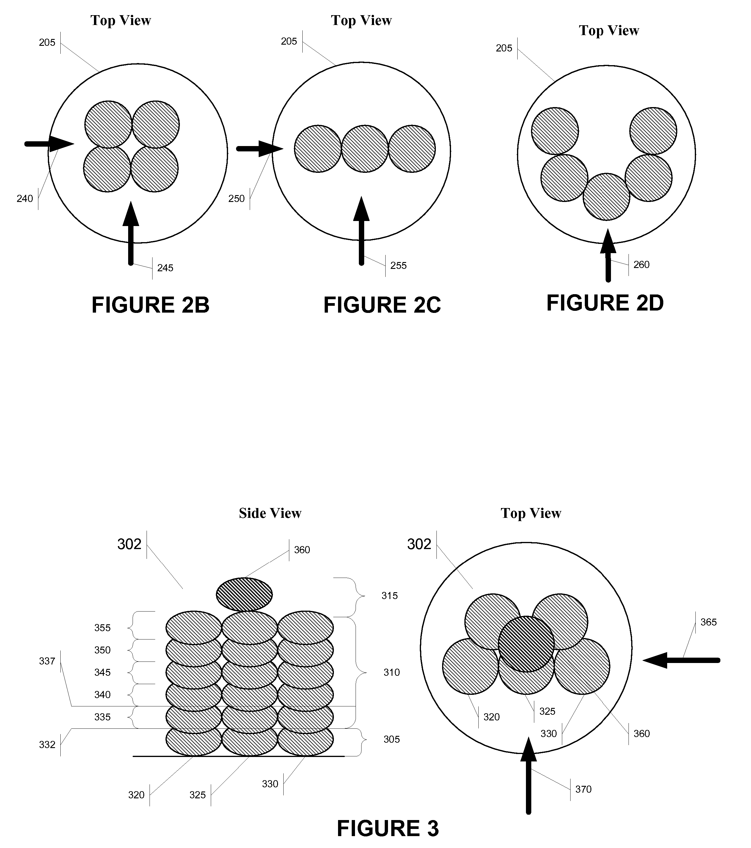
"The present invention provides bump structures that can be formed using SBB techniques. These bumps can be arranged in a buttressed configuration, which allows for substantial height and can support substantial sustained lateral and vertical contact loads. By configuring the bumps in side-by-side contact with one another, an arrangement of individual bumps may be built up to substantially greater height than is possible under current techniques. This arrangement of bumps can be selected to optimize load bearing capacity in any direction or combination of directions. The bumps can be used in a lateral interposer based probe card assembly, semiconductor and / or MEMS packaging, and integrated circuit bound to a PCB."

Problems solved by technology

However, when the die contains few connection points then the die may not have a durable connection to the PCB.
Unfortunately, elevating the die from the surface of the PCB using conventional techniques may result in a connection that suffers from low shear strength; thus is not durable or reliable.
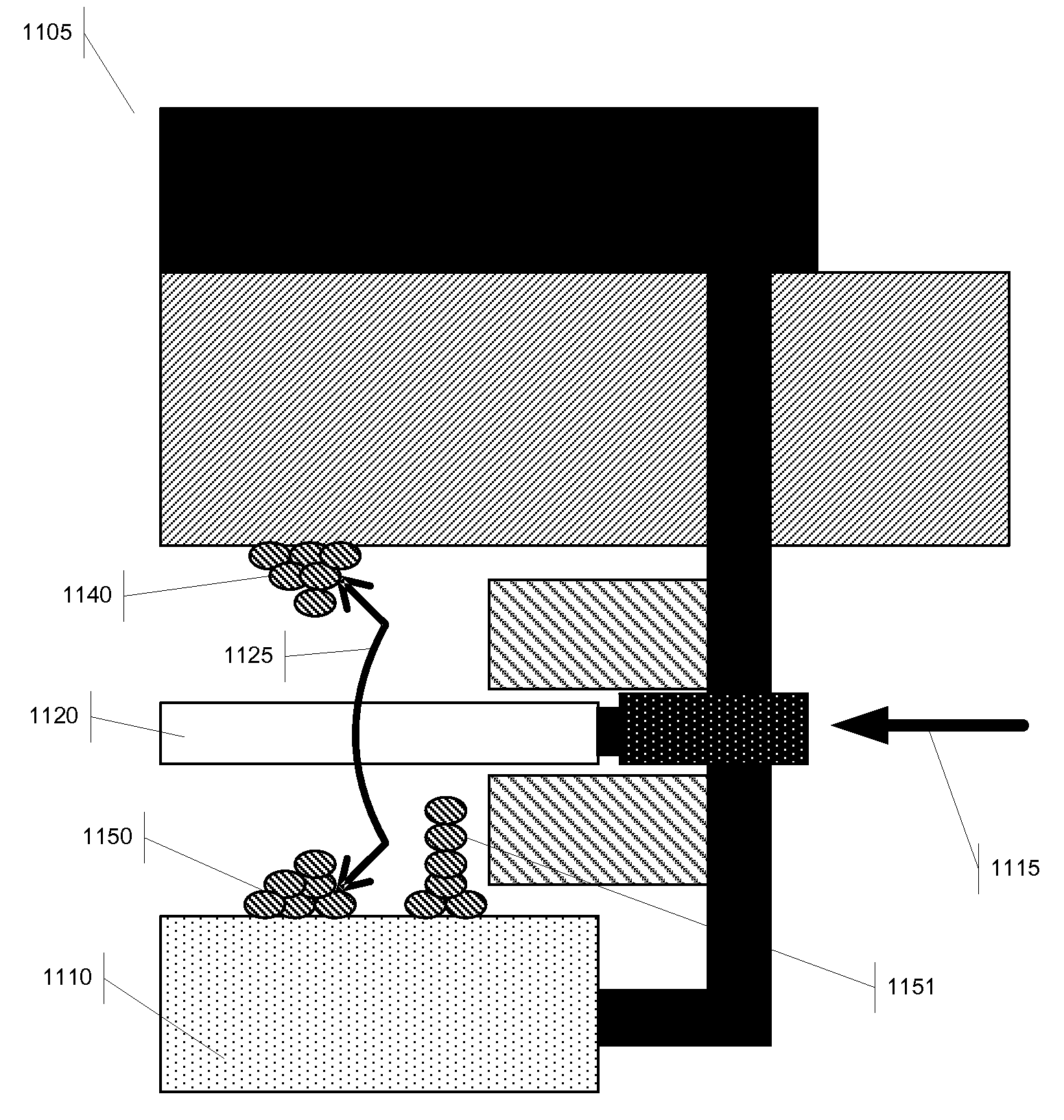
One such probe contactor that may be used is a bump applied by SBB; however, current SBB techniques yield a single bump that may be too short to fully engage the lateral interposer 1105, or yield a column of bumps that is too weak, rendering testing difficult, if not impossible.
These structures, however, have very little lateral strength because they contain a footprint of only one bump; thus in bonding a die to a PCB with such a structure, the connection would not be durable or reliable.
Similarly, the tall structure could not survive the lateral stress exerted by the lateral interposer used in semiconductor testing.

Method used


Image

  • Stacked contact bump
  • Stacked contact bump
  • Stacked contact bump

Examples


Embodiment Construction

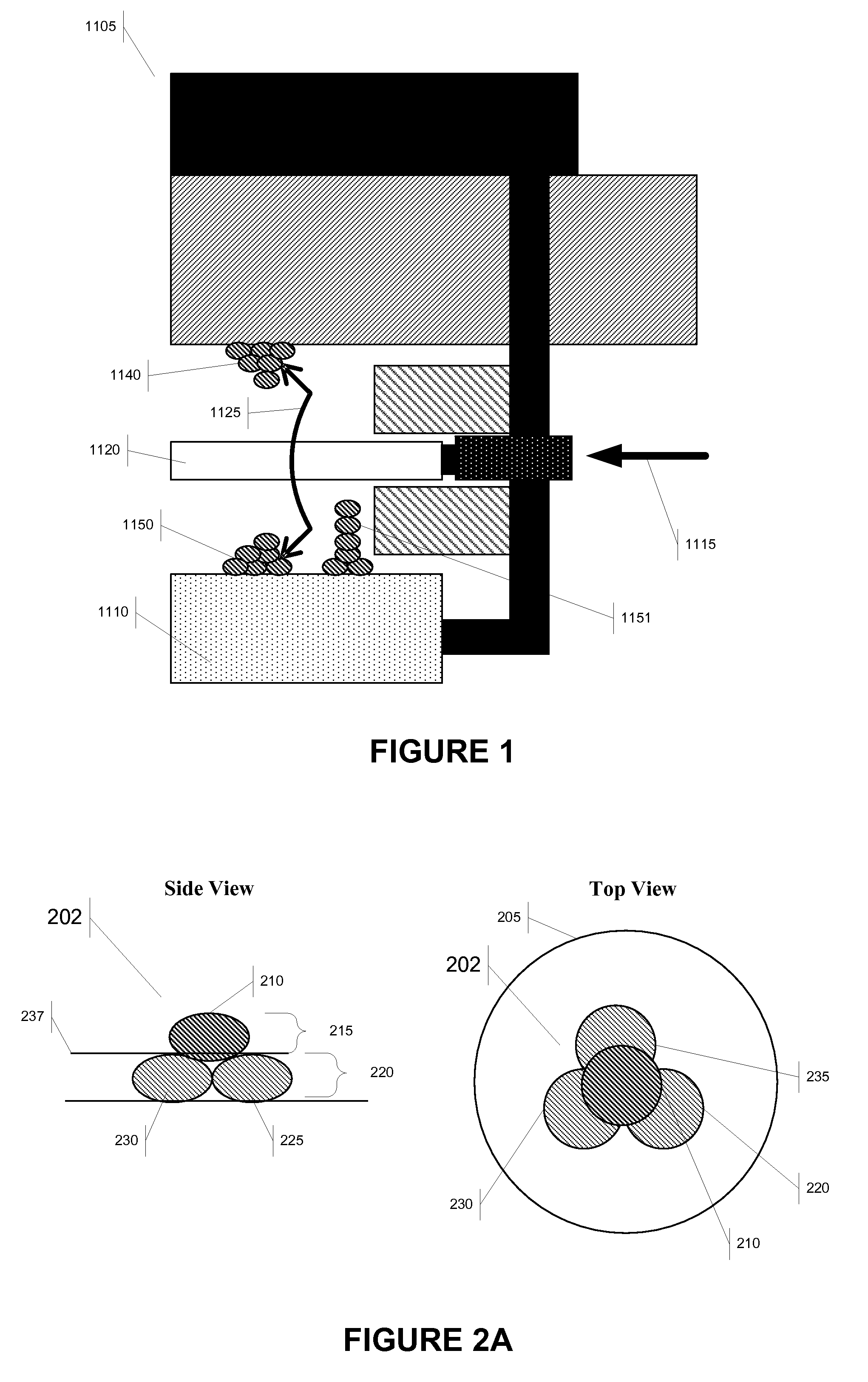
[0029]What is described below are novel bump structures that can be formed by SBB. By arranging the bumps in a buttressed configuration, the bump structure can be built up to a taller height, and is capable of supporting substantial sustained contact loads. FIG. 1 shows one example of an application of the technology described herein. Commonly owned U.S. patent application Ser. No. 11 / 226,568 describes a laterally compliant spring-based interposer 1105 that may be used to test semiconductors. Unlike vertical interposers, the lateral interposer 1105 imparts minimal vertical force on a probe contactor substrate 1110 while the interposer 1105 is engaged. By applying lateral force in the direction of the arrow 1115, the interposer substrate 1120 moves in the direction of the lateral force causing the lateral spring contactor 1125 to come in contact with the probe contactors 1140 and 1150. Probe testing can then be performed because the probe contactor substrate 1110 and the interposer 1...


PUM


Abstract

A novel method for providing bump structures that can be formed by conventional stud bump bonding techniques is disclosed. The bumps can be arranged in a buttressed configuration that allows for substantial lateral and vertical contact loads, and substantial heights. A side-by-side configuration may be used to build a stacked bump contact that is substantially taller and stronger than is possible under current techniques. Other arrangements can be selected to optimize the load bearing capacity in any direction or combination of directions.

Description

RELATION TO A RELATED PATENT APPLICATION[0001]The present patent application is related to U.S. patent application Ser. No. 11 / 226,568 filed on Sep. 14, 2005 by inventors Raffi Garabedian, Nim Tea and Salleh Ismail. The content of this related patent application is incorporated herein by reference.FIELD OF THE INVENTION[0002]The present invention relates to structures formed by stud bump bonding, which may be used in semiconductors and semiconductor wafer testing.BACKGROUND OF THE INVENTION[0003]Selecting the proper method for connecting semiconductor dies to a printed circuit board (PCB) is an important design consideration which may affect the reliability and scalability of the final PCB. One method, that is currently used heavily, is stud bump bonding (SBB). The process of forming SBB is conceptually simple and consists of few steps: forming a free air ball, bonding the ball to the bond pads of the die, and tearing off the wire to provide a free tail bump. The ball (or bump), whi...

Claims


Application Information

Patent Timeline
Patent Type & Authority Patents(United States)
IPC IPC(8): H01L23/48
CPCG01R3/00H01L24/12H01L24/72G01R1/06733H01L2224/1134H01L2224/1308H01L2224/13144H01L2224/13147H01L2224/13164H01L2224/13169H01L2924/01004H01L2924/0102H01L2924/01025H01L2924/01027H01L2924/01029H01L2924/01046H01L2924/01057H01L2924/01074H01L2924/01078H01L2924/01079H01L2924/01082H01L2924/01327H01L2924/14H01L2924/00014H01L2924/00013H01L2924/01023H01L2924/01033H01L2224/13099H01L2224/05552
Inventor YABUKI, RICHARDTEA, NIM
Owner ADVANTEST AMERICA
Learn More