Semiconductor device and semiconductor device manufacturing method

Inactive Publication Date: 2008-01-24
PANASONIC CORP
View PDF4 Cites 32 Cited by
  • Summary
  • Abstract
  • Description
  • Claims
  • Application Information

AI Technical Summary

Benefits of technology

[0011]In the case where a layered film composed of insulating films including different metal elements is formed by one film formation system, however, pealing off of a film from the reaction pipe

Problems solved by technology

In the case where a layered film composed of insulating films including different metal elements is formed by one film formation system, however, pealing off of a film from the reaction pipe an

Method used


Image

  • Semiconductor device and semiconductor device manufacturing method
  • Semiconductor device and semiconductor device manufacturing method
  • Semiconductor device and semiconductor device manufacturing method

Examples


embodiment 1

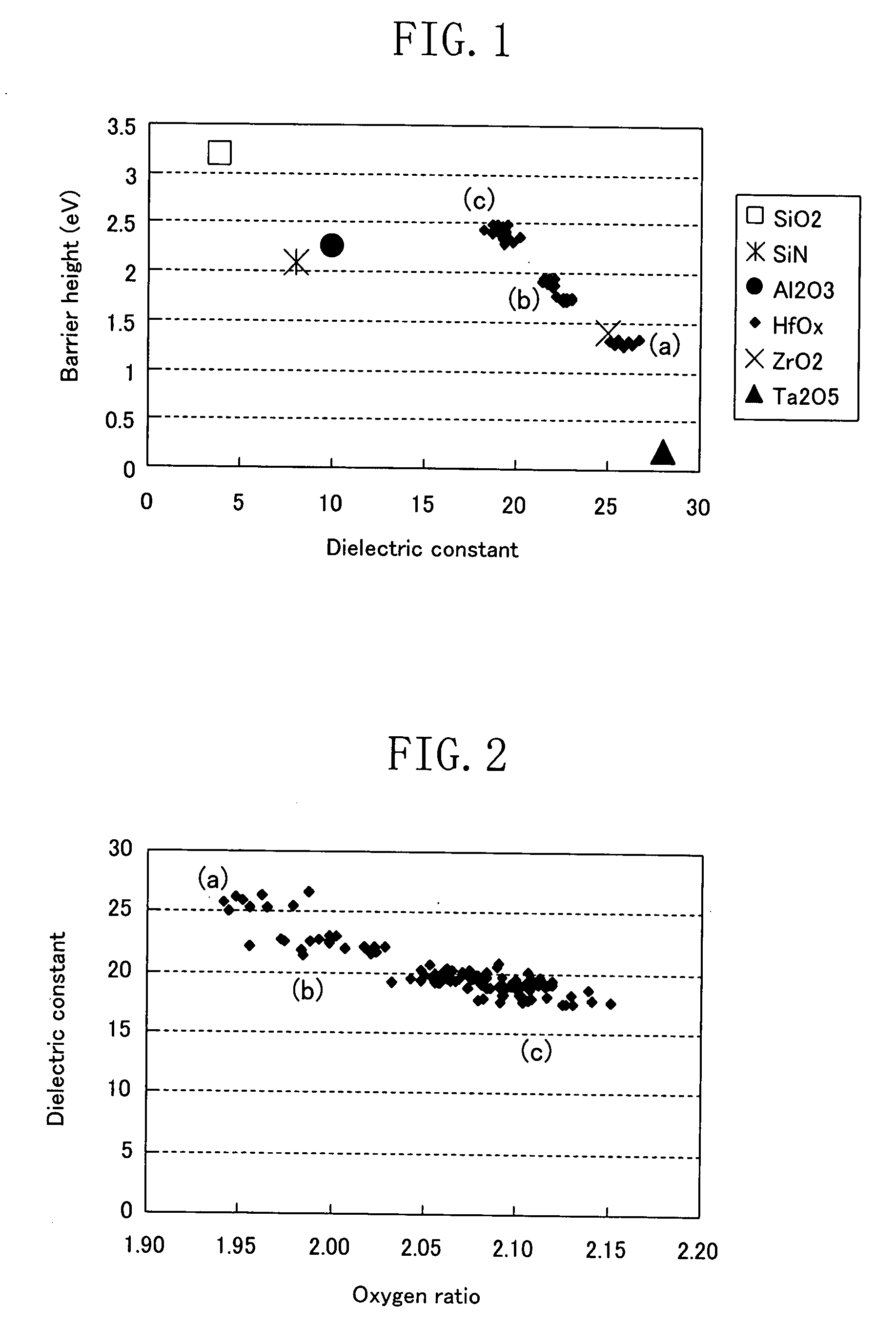
[0043]FIG. 1 is a graph showing a relationship between the dielectric constant (relative dielectric constant) and the barrier height of hafnium oxide films having different barrier heights in the present invention. In FIG. 1, (a) indicates a conventional hafnium oxide film having a dielectric constant of 25 to 28 and a barrier height of approximately 1.4 V while (b) and (c) indicate hafnium oxide films having greater barrier heights than (a). The barrier height of the hafnium oxide film (c), is approximately 2.4 to 2.5 eV, which is greater than the barrier heights of an Al2O3 film and a silicon nitride film (SiN), and in addition, the dielectric constant thereof is higher than the dielectric constants of an Al2O3 film and a silicon nitride film (SiN). As shown in FIG. 1, the hafnium oxide films of the present invention show a tendency that the dielectric constants thereof lowers as the barrier heights thereof are increased.

[0044]FIG. 2 is a graph showing a relationship between the o...

embodiment 2

[0070]While the layered film of the hafnium oxide films having different oxygen ratios are formed by ALD or CVD in Embodiment 1, Embodiment 2 describes another method for forming a layered film of hafnium oxide films having different oxygen ratios, in which one principal face of a hafnium oxide film are subjected to plasma oxidation or hydrogen plasma treatment to change a part of the hafnium oxide film to a region having an oxygen ratio different from the other part.

[0071]FIG. 9A and FIG.9B are sectional view schematically showing a method for fabricating a capacitor including a capacitor insulating film in a three-layered structure composed of hafnium oxide films having different oxygen ratios in the present embodiment.

[0072]First, as shown in FIG. 9A, a hafnium oxide film 102 having a thickness of approximately 2 nm and great barrier height, for example, an oxygen ratio of approximately 2.1 is formed as a first layer on the lower electrode 101 of the capacitor, and then, a hafniu...

embodiment 3

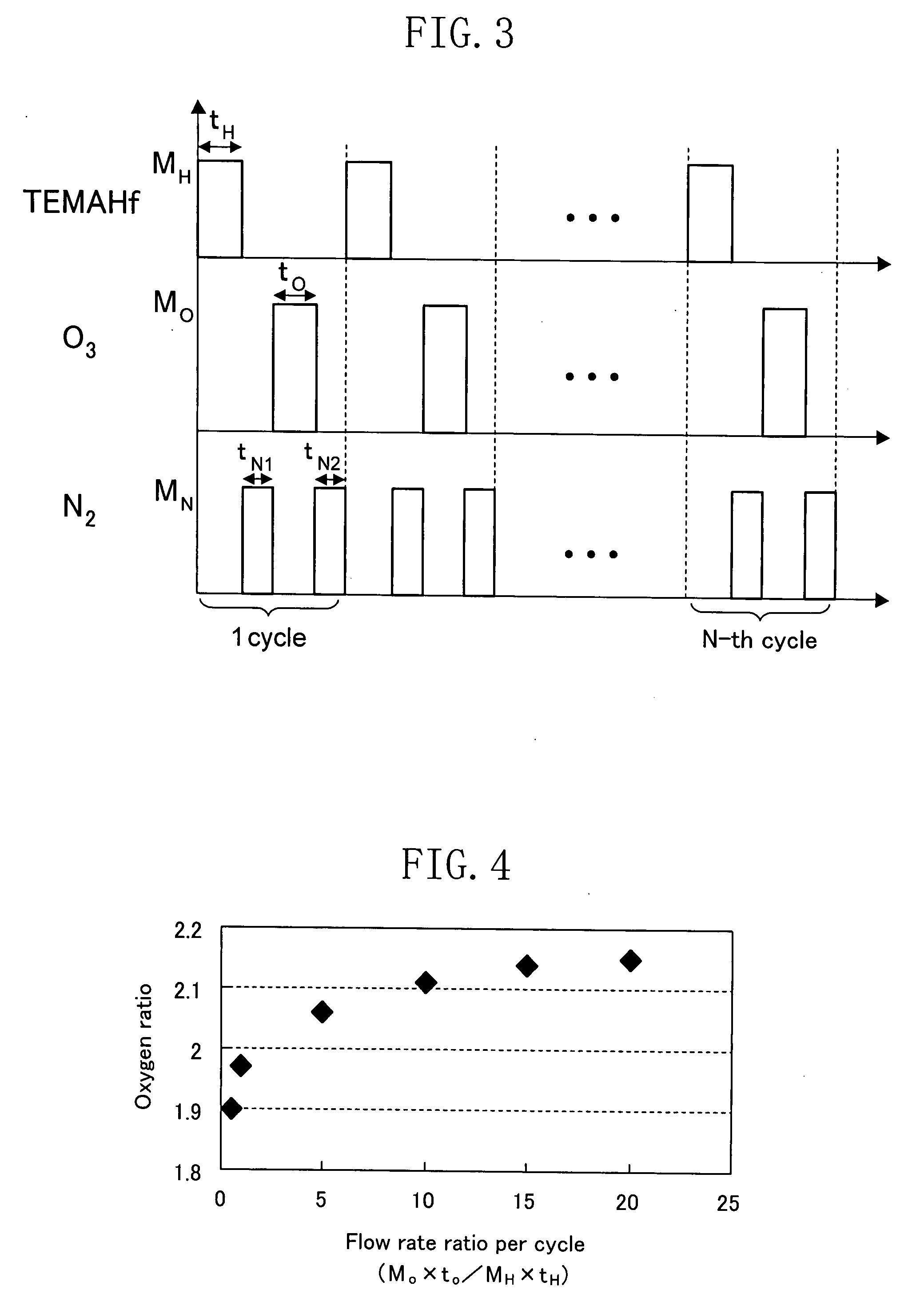
[0083]The present embodiment describes a method for forming a layered film of hafnium oxide films having different oxygen ratios by ALD or CVD, as a modified example of Embodiment 1.

[0084]FIG. 12 is a diagram showing a construction of a semiconductor substrate treatment system in the present embodiment which includes a reaction furnace 204 and a pre-heating chamber 202 for thermal decomposition of TEMAHf as a hafnium source gas before it is supplied to the reaction furnace 204.

[0085]FIG. 13A and FIG. 13B shows the carbon concentration and the oxygen ratio of a hafnium oxide film, respectively, with respect to thermal decomposition temperature of the pre-heating chamber 202. As shown in FIG. 13A and FIG. 13B, the oxygen ratio less depends on the thermal decomposition temperature while the carbon concentration lowers exponentially as the thermal decomposition temperature is increased.

[0086]As also shown in FIG. 14, the film formation rate with respect to the thermal decomposition temp...


PUM


Abstract

A capacitor insulating film composed of a layered film of first- to third-layer hafnium oxide films is formed on a lower electrode of a capacitor. The first- and third-layer hafnium oxide films have a composition ratio of oxygen to hafnium higher than the second-layer hafnium oxide film. Thus, the capacitor insulating film is composed of the first- and third-layer hafnium oxide films having greater barrier height and the second-layer hafnium oxide film having a higher dielectric constant, thereby attaining a capacitor having less leakage current and large capacity.

Description

BACKGROUND OF THE INVENTION[0001]1. Field of the Invention[0002]The present invention relates to semiconductor devices including a dielectric thin film as an element and methods for manufacturing it, and particularly relates to a semiconductor device including a hafnium oxide film as the dielectric thin film and a method for manufacturing it.[0003]2. Description of the Prior Art[0004]In association with recent progress in higher integration, semiconductor devices, such as semiconductor memory devices including capacitive elements for charge accumulation are miniaturized.[0005]For example, in a capacitive structure of a DRAM (dynamic random access memory), a capacitor insulating film is formed between a lower electrode and an upper electrode basically. The cell capacity is in proportion to the dielectric constant of the capacitor insulating film and the effective capacitive area of the two opposed electrodes while being in inverse proportion to the thickness of the capacitor insulati...

Claims


Application Information

Patent Timeline
IPC IPC(8): H01L23/58H01L21/31
CPCH01L21/3141H01L28/40H01L21/31645H01L21/0228H01L21/02252H01L21/022H01L21/0223H01L21/02181
Inventor SUZUKI, JUNYONEDA, KENJIMATSUYAMA, SEIJI
Owner PANASONIC CORP
Why Eureka
Try Eureka