Method for fabricating semiconductor device

a semiconductor device and manufacturing method technology, applied in semiconductor devices, semiconductor/solid-state device details, electrical devices, etc., can solve the problems of oxidation or damage of the cap film b>7/b>, above-mentioned conventional techniques, etc., and achieve the effect of sufficiently reducing the capacitance between the wires

Inactive Publication Date: 2010-06-22
PANASONIC CORP +1
View PDF4 Cites 50 Cited by
  • Summary
  • Abstract
  • Description
  • Claims
  • Application Information

AI Technical Summary

Benefits of technology

[0017]A second problem is that when the part of the insulating film 2 located between the lower wires 6 is etched in the step of FIG. 7A (in the step of forming the air gap grooves 10), a damage layer 13 is formed in the protection film 8 as shown in FIG. 8. When the damage layer 13 is formed as in this case, adhesion between the insulating film 11 deposited in the step illustrated with FIG. 7B and the protection film 8 may be reduced, or the reliability of the device may decrease.
[0019]The present invention is made in view of the above-mentioned problems of the conventional technique. An object of the present invention is to provide a method for fabricating a semiconductor device which realizes a high yield and in which the capacitance between wires can be sufficiently reduced by an air gap.
[0021]According to the method for fabricating the semiconductor device of the present invention, the hard mask film is formed on the protection film, and thus the resist mask used for patterning the hard mask film can be removed with the wire or its cap film (diffusion prevention film) being covered with the protection film, in other words, with the wire or its cap film not being exposed. Therefore, oxidation of the wire or its cap film in resist removal or subsequent polymer removal can be prevented, so that it is possible to prevent a reduction in yield.
[0024]As described above, the present invention relates to a method for fabricating a semiconductor device. Especially, when the present invention is applied to a technique for forming an air gap between wires, the fabrication yield of a semiconductor device in which capacitance between the wires can sufficiently be reduced by the air gap is improved, and thus the present invention is very useful.

Problems solved by technology

However, the above-mentioned conventional technique has problems as follows.
A first problem is that when the resist mask 9 used in the step of FIG. 6C (in the step of removing the protection film 8) is removed or when a polymer is removed, the cap film 7 is oxidized or damaged as illustrated with FIG. 8.
A third problem is that the resist mask 9 which is used in the step of FIG. 6C (in the step of removing the protection film 8) and in the step of FIG. 7A (in the step of forming the air gap grooves 10) does not have sufficient etching resistance.
That is, when a resist film thickness sufficient for removing the protection film 8 and the insulating film 2 between the wires can not be ensured, the resist mask 9 is etched away during etching of the insulating film 2 between the wires, so that the protection film 8 is etched, which may lead to a reduction in reliability of the device.

Method used


Image

  • Method for fabricating semiconductor device
  • Method for fabricating semiconductor device
  • Method for fabricating semiconductor device

Examples


embodiment 1

[0033]A method for fabricating a semiconductor device according to Embodiment 1 of the present invention will be described below with reference to the drawings.

[0034]FIGS. 1A through 1D, FIGS. 2A through 2D, and FIGS. 3A through 3D are cross-sectional views illustrating respective steps in the method for fabricating the semiconductor device according to Embodiment 1.

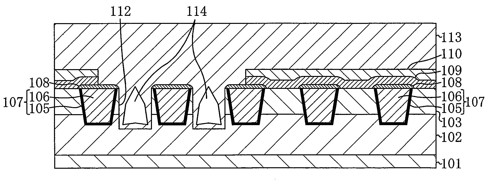
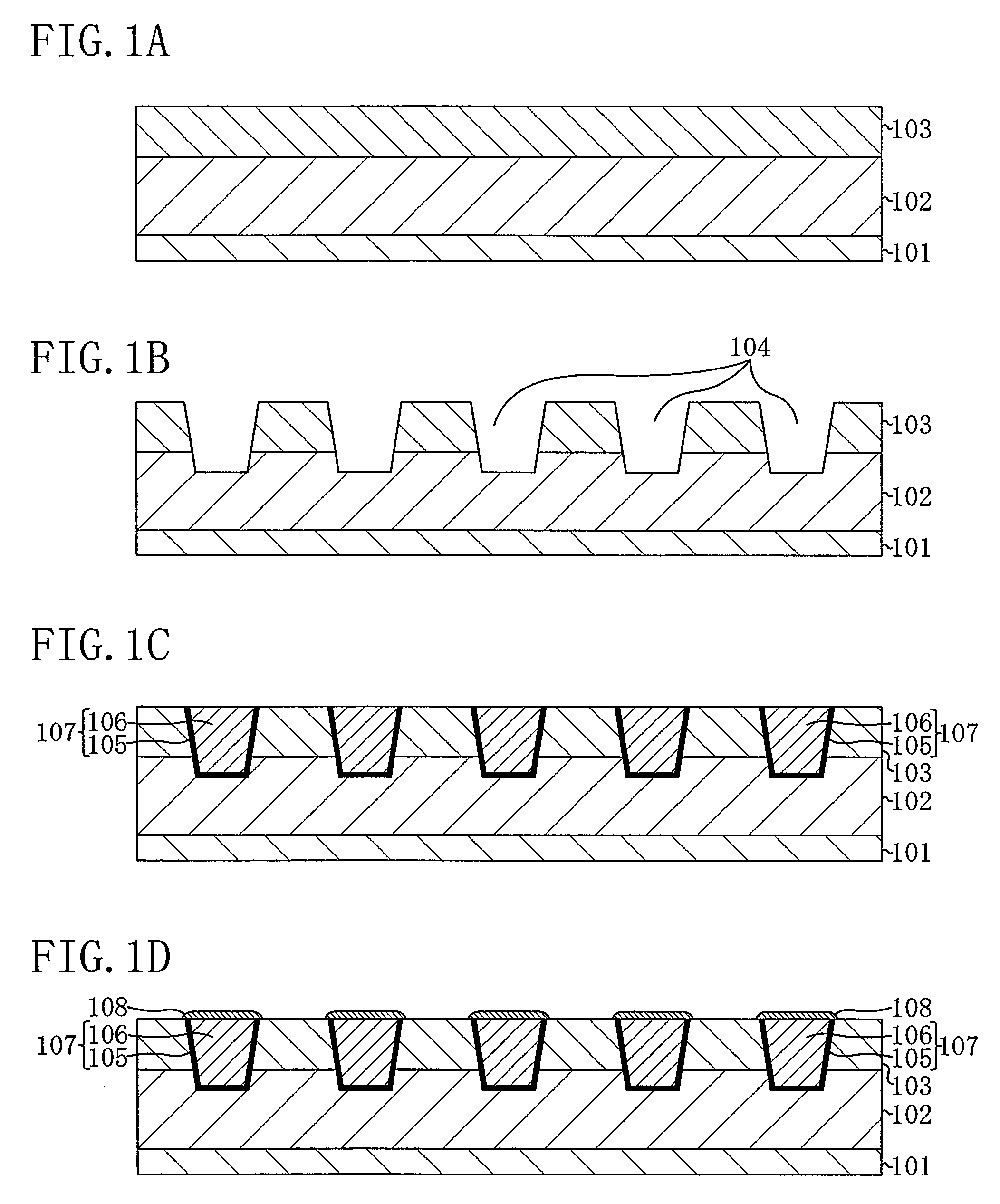
[0035]First, as illustrated with FIG. 1A, over a semiconductor substrate 101, an inter-layer insulating film 102 and an inter-wire insulating film 103 are formed. It is to be noted that in the present embodiment, as the inter-layer insulating film 102, for example, a SiOC film is used, and as the inter-wire insulating film 103, for example, a TEOS (tetraethylorthosilicate) film is used.

[0036]Then, as illustrated with FIG. 1B, photolithography and dry etching are performed to form wiring grooves 104 which penetrate through the inter-wire insulating film 103 and reach inside the inter-layer insulating film 102.

[0037]Then, ...

embodiment 2

[0058]A method for fabricating a semiconductor device according to Embodiment 2 of the present invention will be described below with reference to the drawings. It is to be noted that descriptions as to Embodiment 2 are given of only different points from Embodiment 1 described above, and the same descriptions as those of Embodiment 1 are not repeated.

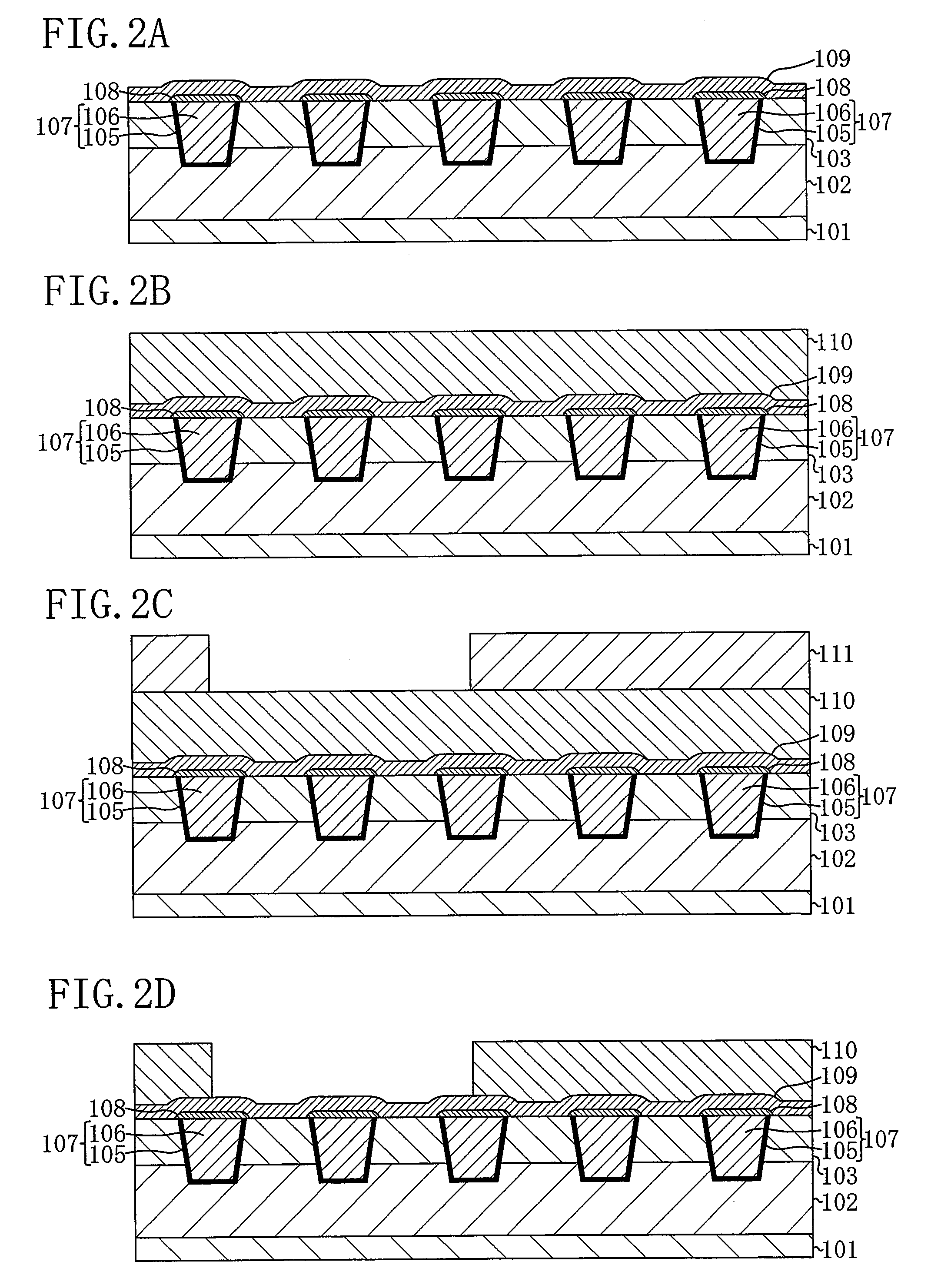
[0059]FIG. 4A is a cross-sectional view illustrating a step of the method for fabricating the semiconductor device according to Embodiment 2. The present embodiment is different from Embodiment 1 in that between the step of forming the air gap grooves 112 of FIG. 3C and the step of forming the air gaps 114 of FIG. 3D (the step of forming the inter-layer insulating film 113), the hard mask film 110 is removed by wet etching or the like as illustrated with FIG. 4A. This makes it possible to directly deposit the inter-layer insulating film 113 on the protection film 109 in the step of forming the air gaps 114 of FIG. 3D. Therefore, it is ...


PUM


Abstract

After a first insulating film is formed on a substrate, a wiring groove is formed in the first insulating film, and then a wire is formed inside the wiring groove. Subsequently, a protection film is formed on the first insulating film and on the wire, and then a hard mask film is formed on the protection film. After that, the hard mask film is patterned. Subsequently, the protection film and the first insulating film are partially removed using the patterned hard mask film to form an air gap groove, and then a second insulating film is formed to close an upper portion of the air gap groove for forming an air gap.

Description

BACKGROUND OF THE INVENTION[0001]1. Field of the Invention[0002]The present invention relates to a method for fabricating a semiconductor device.[0003]2. Description of the Prior Art[0004]Progressing miniaturization of semiconductor integrated circuit device in recent years narrows a wire-to-wire spacing. This results in a problem that capacitance between wires increases, lowering the propagation velocity of a signal. To reduce the capacitance between the wires, it has been studied to embed an insulating film material having a low dielectric constant between the wires. Meanwhile, it has also been studied to form an air gap between the wires to reduce the capacitance between the wires. A conventional method for forming the air gap disclosed in Patent Document 1 will be described below with reference to the drawings.[0005]First, as illustrated with FIG. 5A, on a surface of a semiconductor substrate 1, an insulating film 2 is formed.[0006]Then, as illustrated with FIG. 5B, photolithogr...

Claims


Application Information

Patent Timeline
Patent Type & Authority Patents(United States)
IPC IPC(8): H01L21/302H01L21/461
CPCH01L21/7682H01L23/5222H01L23/53295H01L21/76849H01L2924/0002H01L2924/00
Inventor UEKI, AKIRAHARADA, TAKESHIISHII, ATSUSHI
Owner PANASONIC CORP
Why Eureka
Try Eureka