Extending metal traces in bump-on-trace structures

A technology of bumps and metal traces on traces, which is applied to electrical components, electrical solid devices, circuits, etc., and can solve the problems of increased risk of stripping

Active Publication Date: 2012-08-29
TAIWAN SEMICON MFG CO LTD
View PDF6 Cites 9 Cited by
  • Summary
  • Abstract
  • Description
  • Claims
  • Application Information

AI Technical Summary

Problems solved by technology

However, without a solder mask layer covering the metal traces, the risk of delamination b

Method used


Image

  • Extending metal traces in bump-on-trace structures
  • Extending metal traces in bump-on-trace structures
  • Extending metal traces in bump-on-trace structures

Examples


Embodiment Construction

[0022] The making and using of embodiments of the invention are discussed in detail below. It should be appreciated, however, that the present invention provides many applicable inventive concepts that can be embodied in a wide variety of specific contexts. The specific embodiments discussed are merely illustrative of specific ways to make and use the invention, and do not limit the scope of the disclosure.

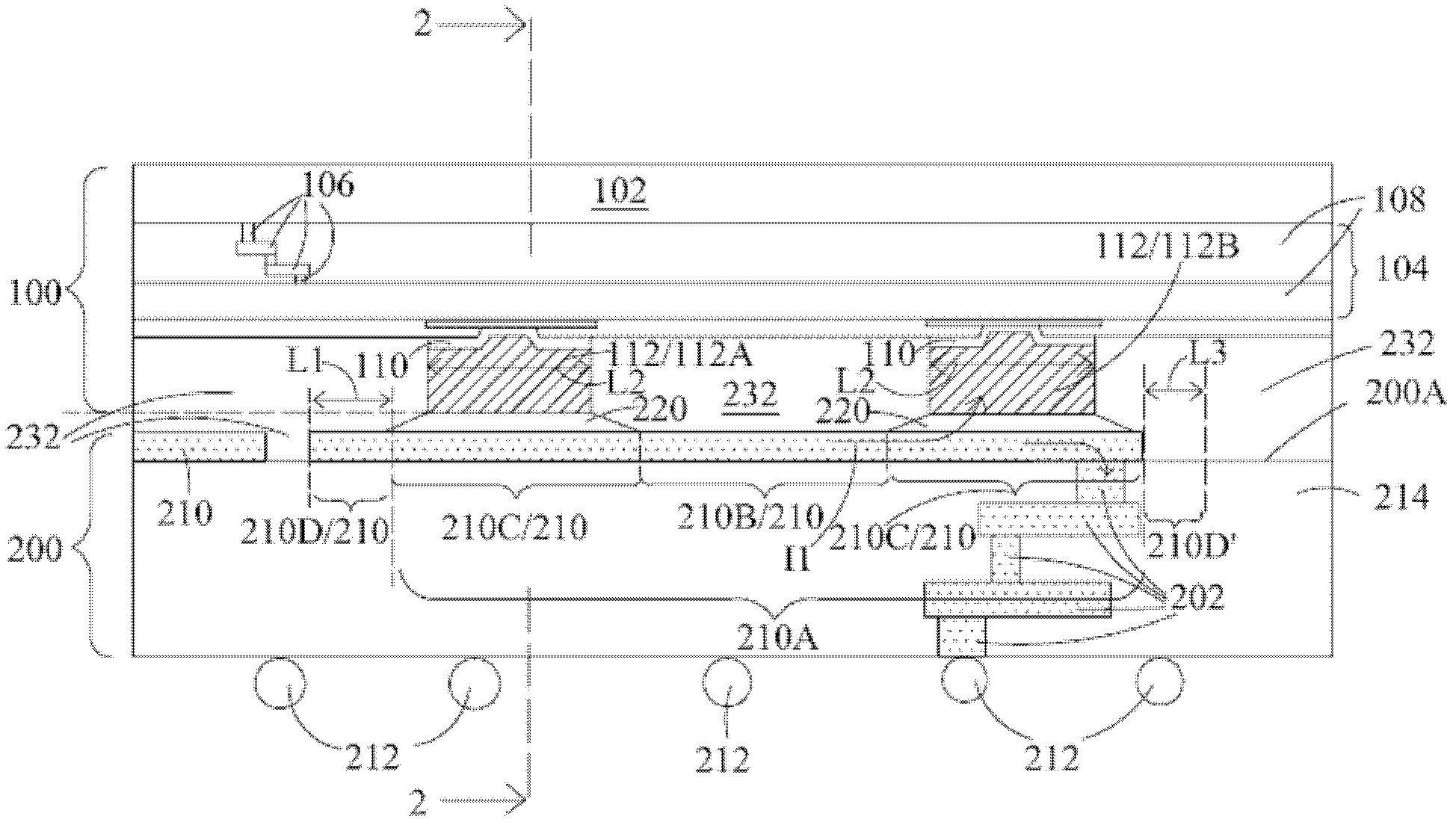
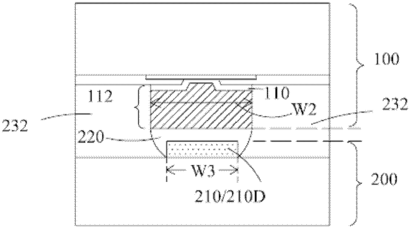
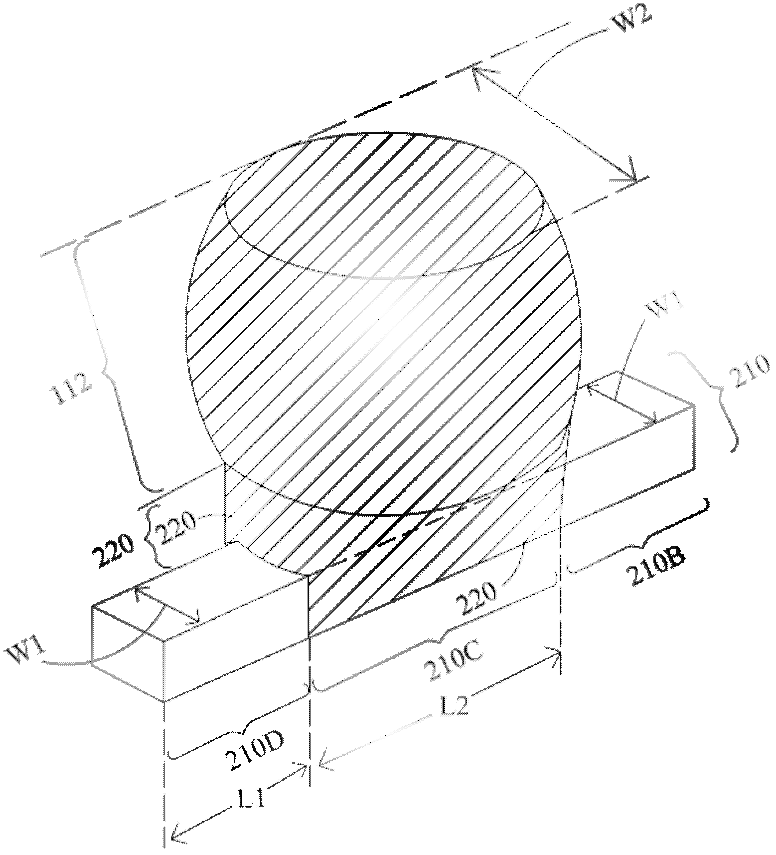
[0023] Package structures including bump-on-trace (BOT) structures are provided according to embodiments. Variations of the embodiments are discussed. Throughout the drawings and described embodiments, the same reference numerals are used to designate the same elements.

[0024] figure 1 A cross-sectional view of a package structure according to an embodiment is shown. The package structure includes: workpiece 100 bonded to workpiece 200 . Workpiece 100 may be a device die including active devices such as transistors (not shown) therein, but workpiece 100 may also be...


PUM

PropertyMeasurementUnit
Lengthaaaaaaaaaa

Abstract

A device includes a work piece, and a metal trace on a surface of the work piece. A Bump-on-Trace (BOT) is formed at the surface of the work piece. The BOT structure includes a metal bump, and a solder bump bonding the metal bump to a portion of the metal trace. The metal trace includes a metal trace extension not covered by the solder bump. The invention also provides extending metal traces in bump-on-trace structures.

Description

technical field [0001] The present invention relates to the field of semiconductors, and more particularly, to a metal trace extending in a bump-on-trace structure. Background technique [0002] Bump-on-trace (BOT) is used in flip-chip packaging where metal bumps are bonded directly to narrower metal traces in the package substrate, large width metal pads. The BOT structure requires a smaller chip area, and the manufacturing cost of the BOT structure is lower. The conventional BOT structure can achieve the same reliability as the conventional bonding structure based on metal pads. [0003] BOT structures often include a solder mask layer formed over the metal traces. The solder mask layer covers portions of the metal traces and leaves certain openings through which the metal traces are exposed. During the bonding process, solder bumps extend into the openings and bond to exposed portions at the metal traces. The solder mask layer provides mechanical support for the BOT ...

Claims


Application Information

Patent Timeline
IPC IPC(8): H01L23/48H01L23/488
CPCH01L24/13H01L2924/01013H01L2924/01029H01L2924/01079H01L2924/01082H01L2924/01019H01L2924/01033H01L2924/01074H01L2924/01322H01L2924/014H01L23/49838H01L24/17H01L2224/13082H01L2224/13147H01L2224/16013H01L2224/16225H01L23/49816H01L2224/131H01L2224/16227H01L2924/00013H01L2224/1308H01L24/16H01L2924/00014H01L2924/00H01L2224/13099H01L2224/13599H01L2224/05599H01L2224/05099H01L2224/29099H01L2224/29599
Inventor 陈玉芬谢玉宸林宗澍普翰屏吴俊毅郭庭豪
Owner TAIWAN SEMICON MFG CO LTD
Why Eureka
Try Eureka