
Imaging device and method of manufacture

a technology of imaging device and manufacturing method, which is applied in the direction of semiconductor device, basic electric element, electrical apparatus, etc., can solve the problems of complicated assembly methods, cumbersome packaging, and inconvenient use of known packages, and achieve the effect of easy removal of finished products

Inactive Publication Date: 2007-01-02
ROUND ROCK RES LLC
View PDF33 Cites 9 Cited by
  • Summary
  • Abstract
  • Description
  • Claims
  • Application Information

AI Technical Summary

Benefits of technology

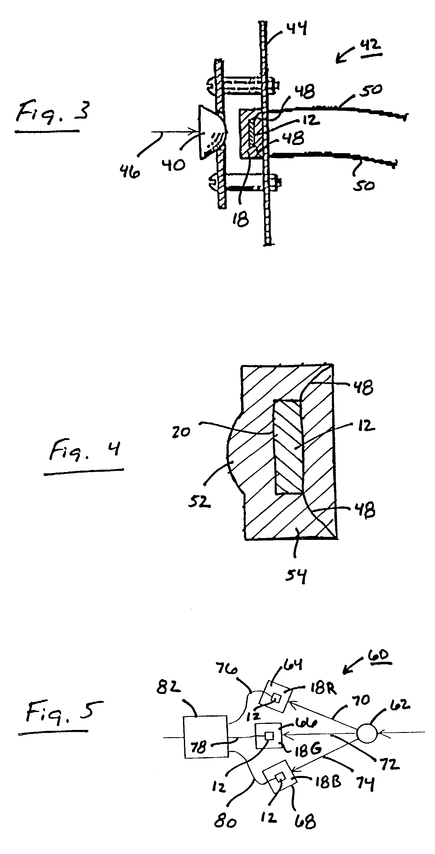
[0014]The present invention also relates to a method of making a packaged imaging device. The method includes the following steps: locating an integrated circuit in a mold; injecting transparent resin into the mold such that the integrated circuit is covered by the resin; curing the resin; and removing the finished product from the mold. In one aspect of the invention, a release agent is applied to the mold for easy removal of the finished product.

Problems solved by technology

Such packages are generally cumbersome and inconvenient, and the materials are relatively expensive.
In addition, the known packages require complicated methods of assembly.
The imaging device needs to be properly aligned in the housing to avoid misalignment with the plate, which could cause optical distortion.
Dust or other contaminants on the imaging device or inside the glass plate could degrade the performance of the device.

Method used


Image

  • Imaging device and method of manufacture
  • Imaging device and method of manufacture
  • Imaging device and method of manufacture

Examples


Embodiment Construction

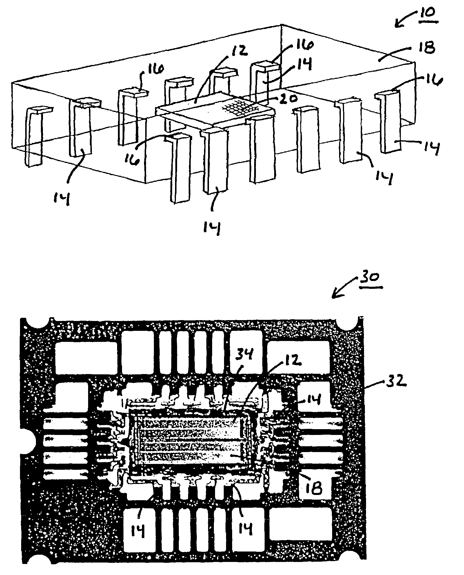
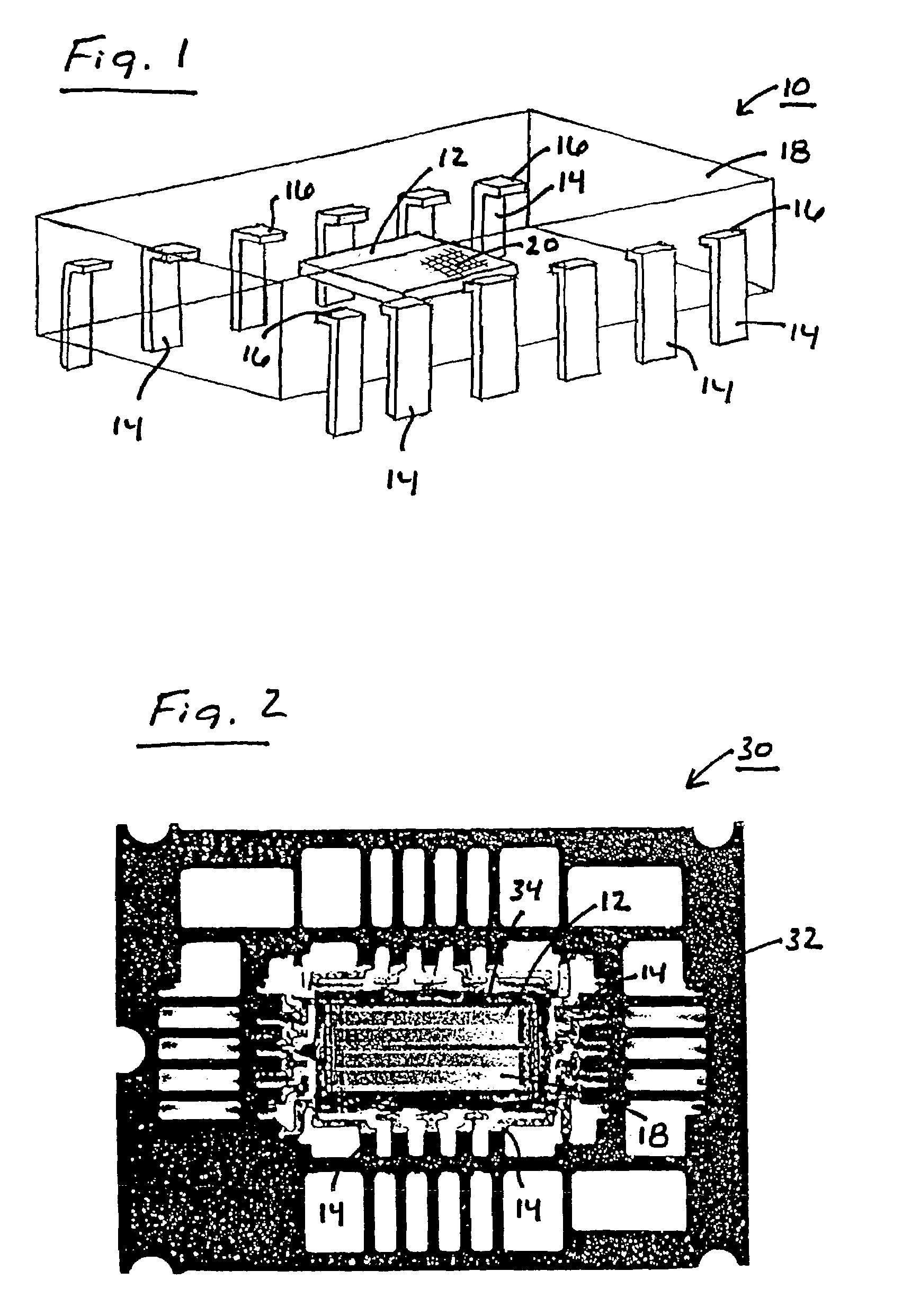
[0029]Referring now to the drawings, where like reference numerals designate like elements, there is shown in FIG. 1 an imaging device 10 constructed in accordance with the present invention. The device 10 has a semiconductor chip 12 and metal leads 14. The inner ends 16 of the leads 14 are connected to the chip 12 by suitable lead wires. The lead wires are not shown in FIG. 1.

[0030]The chip 12, the lead wires, and the inner ends 16 of the leads 14 are completely encapsulated in a transparent plastic package 18. The package 18 provides structural support for the chip 12, the lead wires and the leads 14. In addition, the package 18 protects the chip 12 from the environment. Other features and advantages of the transparent package 18 are described in more detail below.

[0031]The chip 12 may be formed of semiconductor material. The chip 12 may be, for example, a complementary metal oxide semiconductor (CMOS) device. The chip 12 has photosensitive elements 20 for receiving radiant energy...


PUM


Abstract

An imaging chip is packaged in transparent injection molded material. The chip may have photosensitive elements arranged in a two-dimensional array on semiconductor material. Each element corresponds to a pixel of an image. The package may be formed of epoxy resin. In one aspect of the invention, the transparent plastic material provides a color filter. Second and third packages with complementary color filters may be used to provide signals for a color imaging system. In another aspect of the invention, a lens is integrated into the plastic package. In another aspect of the invention, a semiconductor chip is applied to a pre-formed plastic package by bump bonding.

Description

CROSS-REFERENCE TO RELATED APPLICATIONS[0001]This application is a divisional application of U.S. patent application Ser. No. 09 / 090,315, filed Jun. 4, 1998.BACKGROUND OF THE INVENTION[0002]1. Field of the Invention[0003]The present invention relates generally to imaging devices. The invention also relates to methods of packaging such devices. More particularly, the invention relates to a transparent plastic package for supporting and / or protecting a photosensitive semiconductor device.[0004]2. Discussion of the Related Art[0005]Solid-state imaging devices are known in the art. They are used to generate electrical signals representative of an incident image. The devices may be responsive to visible, ultraviolet and / or infrared radiation. The devices may also be used to generate color component signals. Solid-state imaging devices are described in U.S. Pat. No. 5,708,263 (Wong), U.S. Pat. No. 5,461,425 (Fowler et al.) and U.S. Pat. No. 4,441,125 (Parkinson).[0006]Prior art imaging de...

Claims


Application Information

Patent Timeline
Patent Type & Authority Patents(United States)
IPC IPC(8): H01L21/00H01L31/0203
CPCH01L27/14618H01L31/0203H01L27/14683H01L27/14625H01L2924/0002H01L2924/00
Inventor RHODES, HOWARD E.HEITZEBERG, EDWARD J.
Owner ROUND ROCK RES LLC
Learn More