
Bump bonding apparatus and bump bonding method

Inactive Publication Date: 2005-09-08
SHINKAWA CO LTD
View PDF3 Cites 9 Cited by
  • Summary
  • Abstract
  • Description
  • Claims
  • Application Information

AI Technical Summary

Benefits of technology

[0026] The object of the present invention is to provide a bump bonding apparatus and method that has an extremely high reliability in terms of bump formation.

Problems solved by technology

However, since there are numerous unstable elements such as the state of the tip end of the wire, the length of the tail 4a, the bending of the tail 4a, the conditions of alloy debris on the undersurface of the bump 7 stripped from the electrode pad 2 and the like, it is actually difficult to perform a normal evaluation.

Method used


Image

  • Bump bonding apparatus and bump bonding method
  • Bump bonding apparatus and bump bonding method
  • Bump bonding apparatus and bump bonding method

Examples


Embodiment Construction

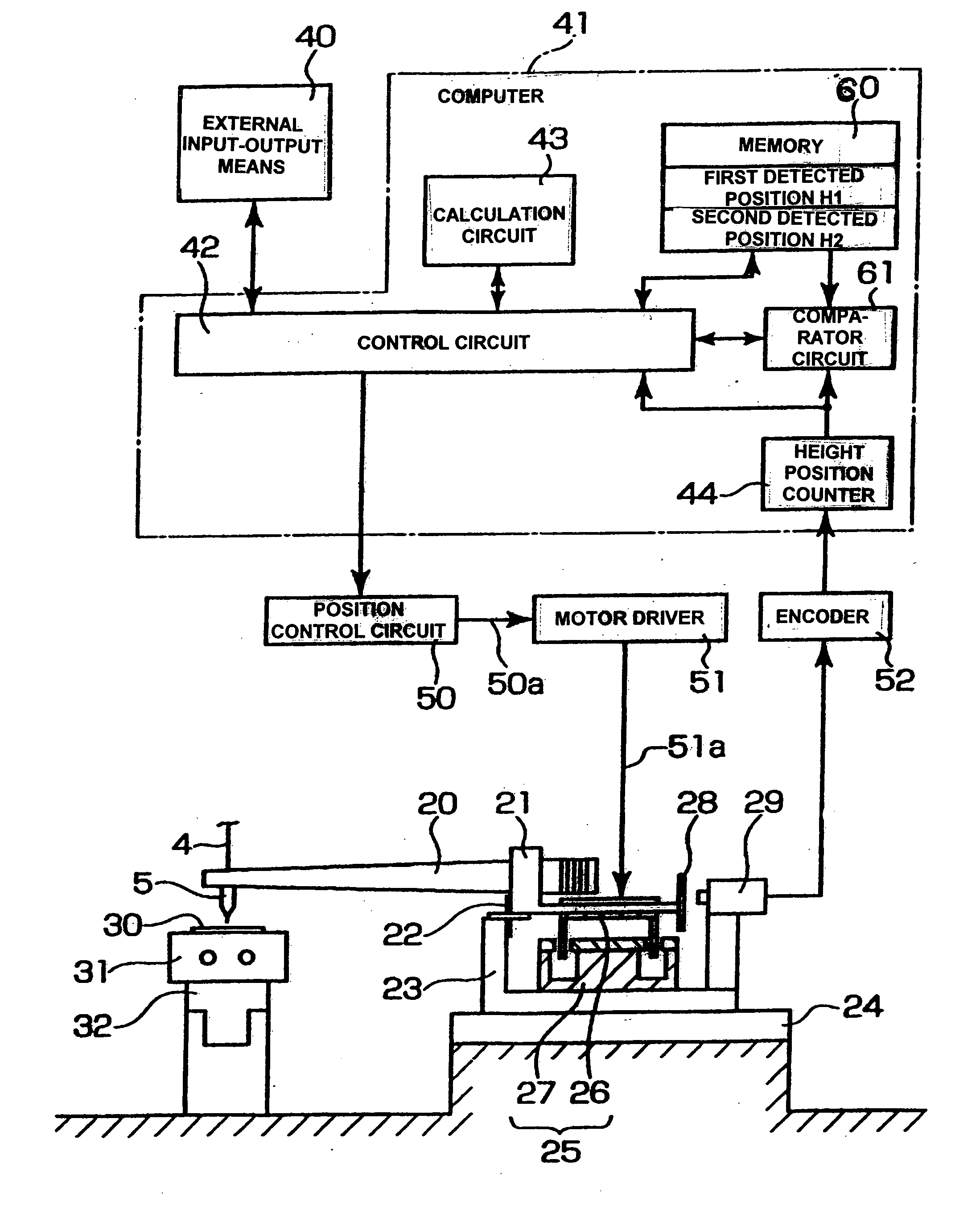
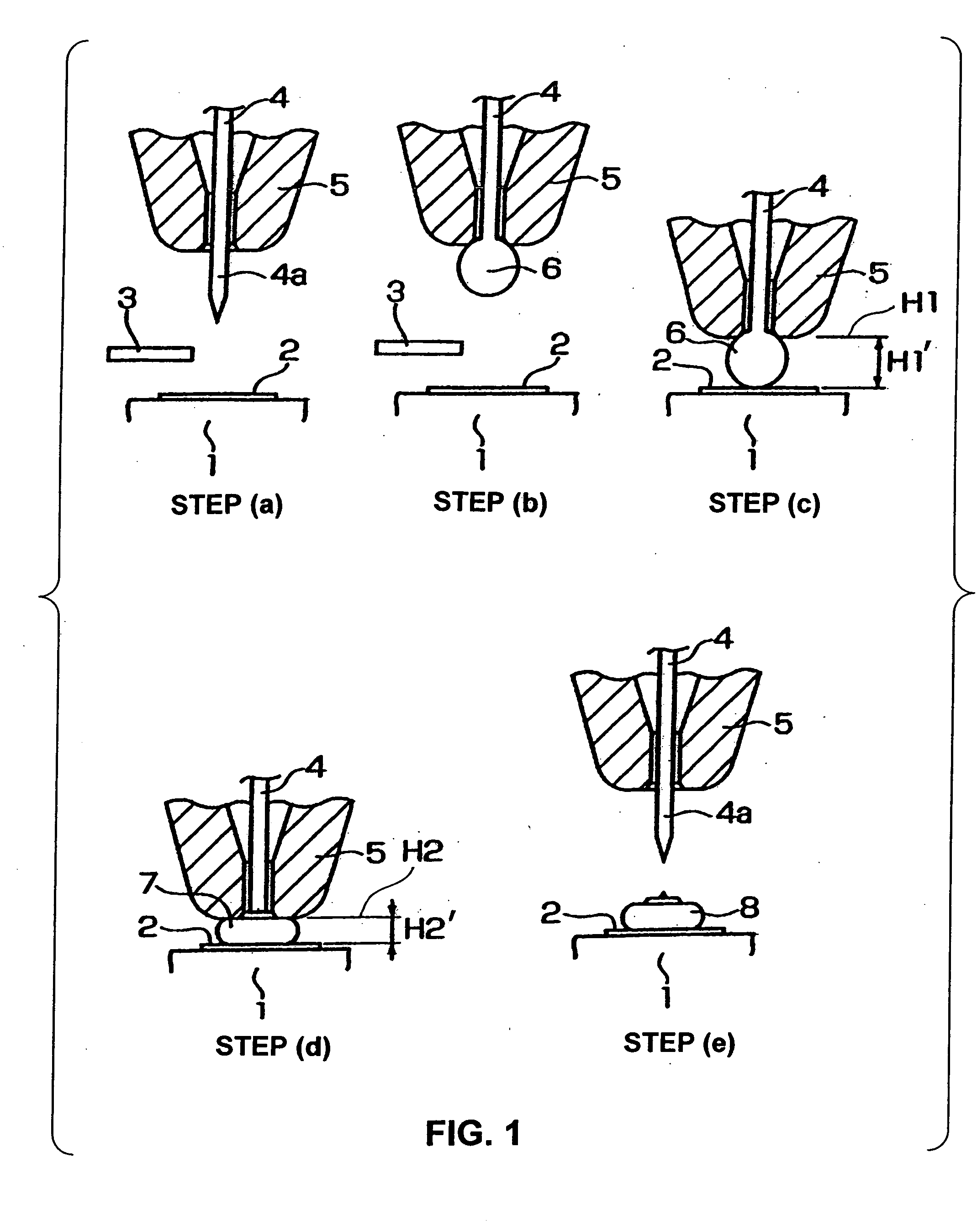
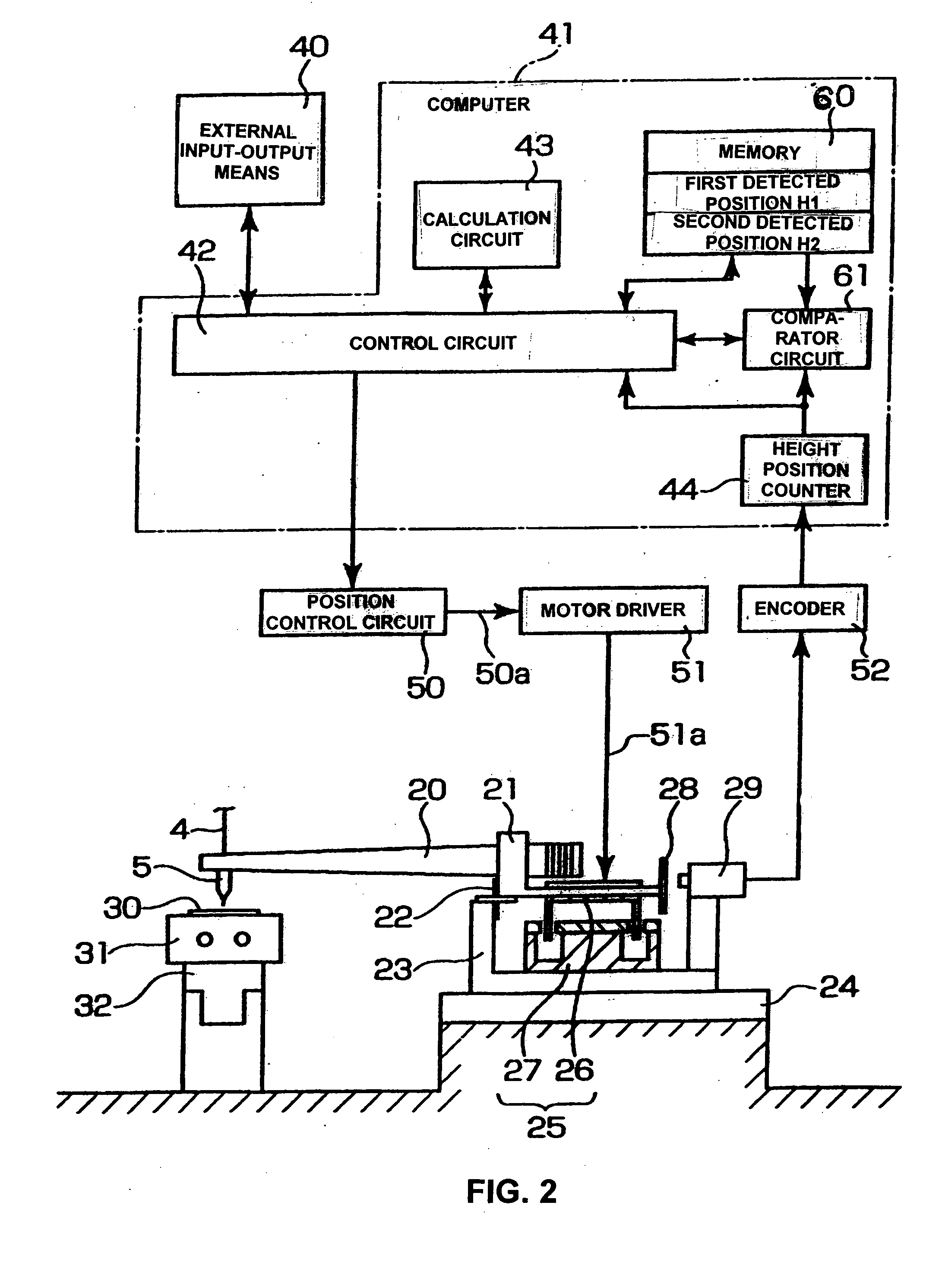
[0046] One embodiment of the present invention will be described with reference to FIGS. 1 through 4. In FIGS. 1 through 4, the same reference numerals are assigned to the members that are the same as those in FIGS. 5 through 7 or that correspond to the members in FIGS. 5 through 7, and a detailed description of such members is omitted.

[0047]FIG. 1 shows the steps (a) through (e) taken in the present invention and corresponds to FIG. 5.

[0048] First, the following work is performed prior to the bump formation. As shown in steps (a) and (b), a ball 6 is formed by performing an electric discharge on the tail 4a of a wire 4 from the discharge electrode 3.

[0049] Next, in step (c), a first detected position H1, which is apart from the surface of the electrode pad with a distance of H1′ and is a contacting level of the ball at the lower end of the capillary 5 at the time when the capillary 5 is lowered and the ball 6 comes into contact with the electrode pad 2, is stored in the memory 6...


PUM


Abstract

A bump bonding apparatus and method in which a ball 6 is formed on the tip end of a wire 4 by an electric discharge between the wire 4 and a discharge electrode 3, and a bump 8 is formed by joining this ball 6 to the pad 2 of a semiconductor chip 1. In cases where the position of the capillary 5, when the capillary 5 is lowered following the next ball formation and the tip end portion of the wire (ball 6 or stripped bump) comes into contact with the electrode pad 2 drops below the lower limit of the permissible error range of the ball contacting level (first detected position H1) of the capillary 5 at a time when a normally formed ball 6, comes into contact with the electrode pad 2, a bump non-adhesion signal is outputted, and the bonding operation is stopped.

Description

BACKGROUND OF THE INVENTION [0001] 1. Technical Field [0002] The present invention relates to a bump bonding apparatus and method that forms a ball on the tip end of a wire passing through a capillary and bonds this ball to a conductor to form a bump. [0003] 2. Description of the Related Art [0004] Bump formation in wire bonding is generally accomplished by the steps (a) through (e) shown in FIG. 5. In FIG. 5, the reference numeral 1 is a semiconductor chip, 2 is an electrode pad that is formed on the surface of the semiconductor chip 1, and 3 is a discharge electrode. [0005] First, in step (a), with a damper (not shown) closed, an electric discharge is made from the discharge electrode 3 onto the tail 4a of a wire 4 that passes through a capillary 5, thus forming a ball 6 on the tip end of the wire in step (b). [0006] Next, in step (c), after the damper (not shown) is opened, the wire 4 is drawn back upward with an appropriate force by means of a back tension mechanism (not shown);...

Claims


Application Information

Patent Timeline
IPC IPC(8): B23K37/00H01L21/60
CPCH01L24/78H01L24/85H01L2224/48463H01L2224/78301H01L2924/01033H01L2924/01006H01L2924/01082H01L2924/01005H01L2224/85148H01L2924/00014H01L2224/85205H01L24/11H01L24/13H01L2224/1134H01L2224/05573H01L2224/05568H01L24/48H01L2224/45099H01L2224/05599H01L2924/00
Inventor TAKAHASHI, KUNIYUKIKATO, FUMIHIKO
Owner SHINKAWA CO LTD
Learn More