Optical modulator

a technology of optical modulators and optical beams, applied in the field of optical modulators, can solve the problems of stray light, confined to the substrate, deterioration of the s/n ratio of output light, etc., and achieve the effect of effectively removing stray light and easy form of stray light removing members

Active Publication Date: 2007-03-08
SUMITOMO OSAKA CEMENT CO LTD
View PDF3 Cites 30 Cited by
  • Summary
  • Abstract
  • Description
  • Claims
  • Application Information

AI Technical Summary

Benefits of technology

[0011] The present invention provides an optical modulator using a thin plate capable of improving an S / N ratio of an output light.

Problems solved by technology

However, in a case where an optical modulator using an LN substrate fabricated in the related art is compared with an optical modulator using a thin LN substrate, as the thickness of the substrate is reduced, the light radiating or leaking from an optical waveguide or the light from an incident optical fiber to a region excluding the optical waveguide (hereinafter, referred to as stray light) has a tendency to be confined to the substrate.
As a result, the S / N ratio of the output light deteriorates.
Moreover, in a case where a thin plate is used for the optical modulator, since a sufficient mechanical strength cannot be obtained by using the thin plate, there is a need to attach the second substrate, that is, a reinforcement plate to the first substrate, that is, the thin plate by using an adhesive or the like as described above.

Method used


Image

  • Optical modulator
  • Optical modulator
  • Optical modulator

Examples


examples

[0065] Now, examples of the optical modulator according to the present invention and test thereof will be described.

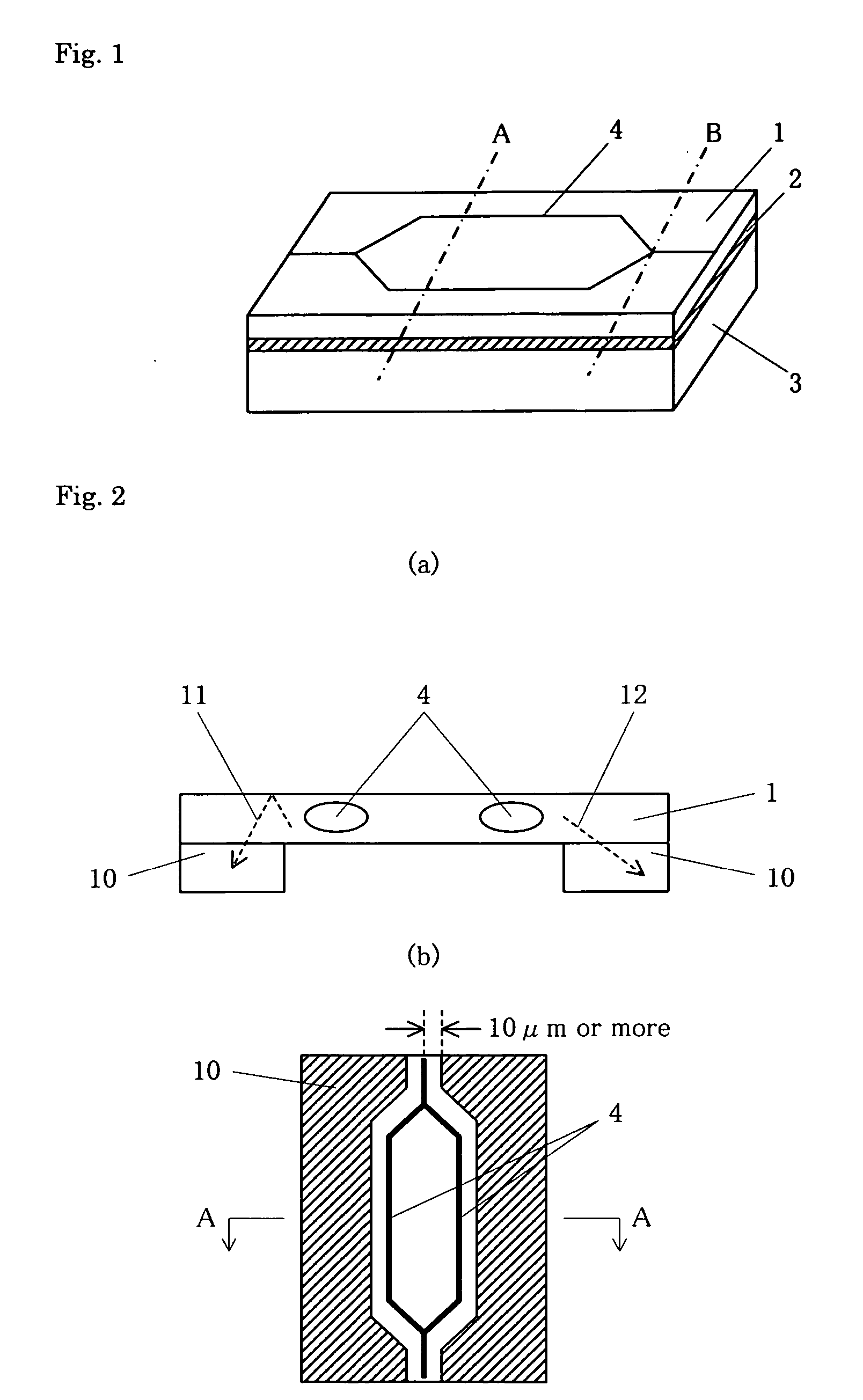
[0066] In order to fabricate a thin-plate optical modulation device, an X-cut LN substrate having a thickness of 500 μm is used. As shown in FIG. 1, a Mach-Zehnder type optical waveguide is formed on a top surface of the substrate by using a Ti diffusion process or the like.

[0067] A thermo-plastic resin is coated on the top surface of the substrate, and a dummy substrate for polishing is attached. A bottom surface of the substrate is polished with a polishing machine to allow a thickness thereof to be 20 μm, and after that, a modulation electrode having a height of 14 μm is formed by using a plating process, so that a thin plate where the optical modulation device is formed is completed.

first example

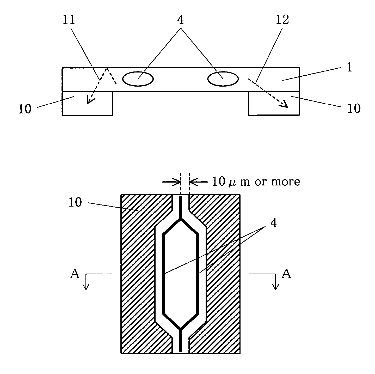
[0068] In a first example, in the bottom surface of the thin plate fabricated by the above-described method, an Al film is formed as a light absorbing member on all the regions which are separated by 10 μm from a region in which the optical waveguide is formed as shown in FIG. 2B. After that, an optical path coupling UV-curable adhesive which has a function of propagating an optical wave in a communication wavelength range is coated, and a substrate made of the same material as the thin plate is attached as a reinforcement plate on the bottom surface of the thin plate.

second example

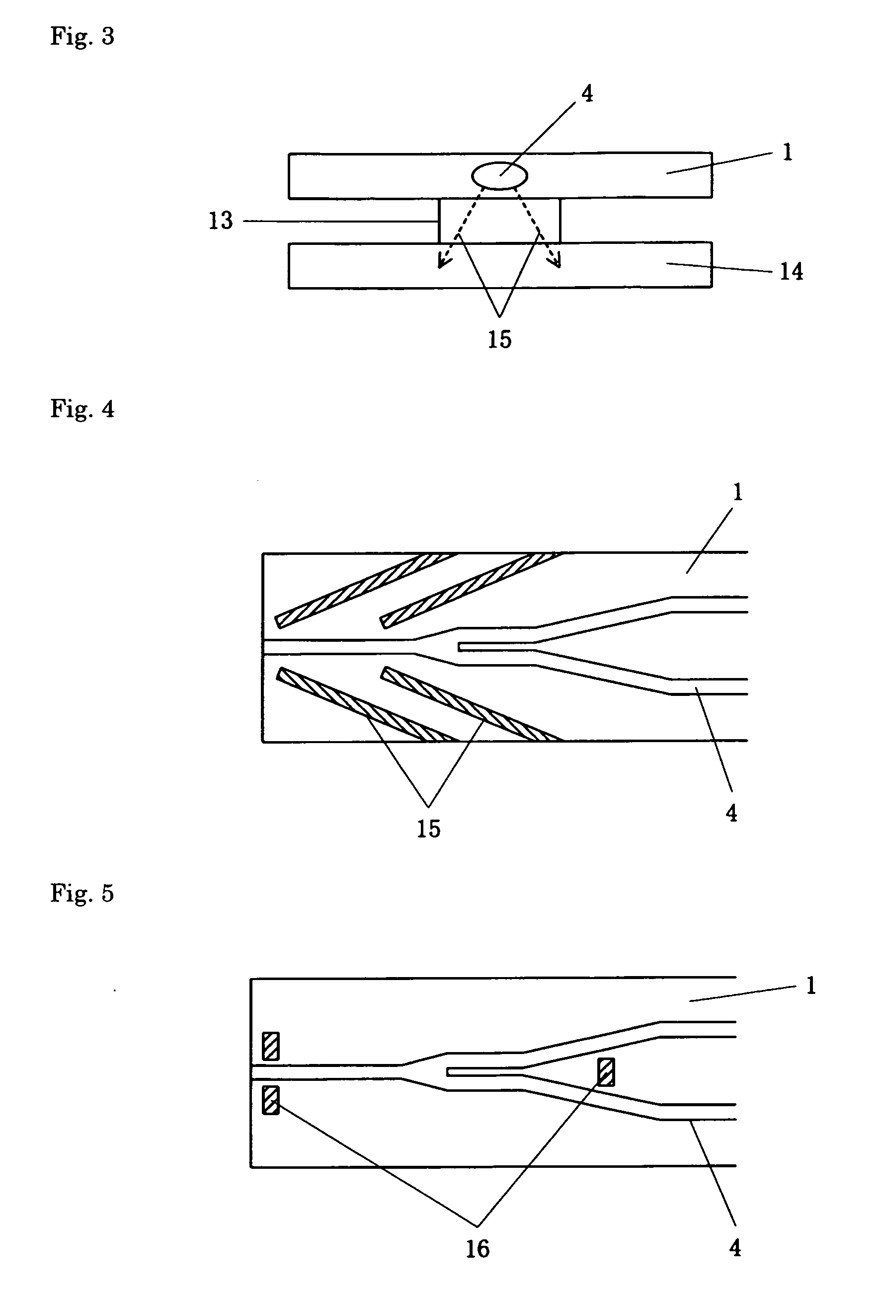
[0069] In a second example, in the bottom surface of the LN thin plate fabricated by the above-described method, a high refractive index portion having a height of 60 μm is disposed in a region where a multiplexing unit of the branch optical waveguide is formed as shown in FIG. 3. The optical path coupling UV-curable adhesive is coated, and a reinforcement plate is attached on the bottom surface of the high refractive index portion. Preferably, the refractive index of the high refractive index portion or the reinforcement plate is equal to or larger than that of the thin plate. In the second example, the high refractive index portion and the reinforcement plate are made of LN which is the same material for the thin plate.


PUM

PropertyMeasurementUnit
thicknessaaaaaaaaaa
thicknessaaaaaaaaaa
thicknessaaaaaaaaaa

Abstract

An optical modulator using a thin plate capable of improving an S / N ratio of an output light is provided. The optical modulator including a thin plate 1 having an electrooptic effect and having a thickness of 20 μm or less, an optical waveguide 4 formed on a top or bottom surface of the thin plate, and a modulation electrode formed on the top surface of the thin plate to modulate light passing through the optical waveguide, wherein a stray light removing member 10 is disposed within the thin plate or in a vicinity of the thin plate.

Description

BACKGROUND OF THE INVENTION [0001] 1. Field of the Invention [0002] The present invention relates to an optical modulator, and more particularly, to an optical modulator using a thin plate having an electrooptic effect. [0003] 2. Related Art Statement [0004] In the related art, waveguide type optical modulators having optical waveguides or modulation electrodes formed on a substrate having an electrooptic effect have been widely used for optical communication fields or optical measurement fields. [0005] Particularly, an amount of information transmission increases as multimedia technology is developed. Therefore, there is a need for a wide frequency band modulation technology in an optical modulator. In order to implement the wide frequency band modulation, various external modulation schemes with an LN (lithium niobate) modulator or the like are used. However, in order to implement the wide frequency band modulation with the LN modulator, there is a need for velocity matching betwe...

Claims


Application Information

Patent Timeline
Patent Type & Authority Applications(United States)
IPC IPC(8): G02F1/035
CPCG02F1/0311G02F2201/08G02F1/225G02F1/035
Inventor ICHIOKA, MASAYUKIKONDOU, KATSUTOSHIISHIKAWA, YASUHIROSHINRIKI, TAKASHIOIKAWA, SATOSHIICHIKAWA, JUNICHIRO
Owner SUMITOMO OSAKA CEMENT CO LTD
Why Eureka
Try Eureka