

Extended deposition range by hot spots
a hot spot and deposition range technology, applied in the direction of chemical vapor deposition coating, metallic material coating process, coating, etc., can solve the problem of losing the self-terminating nature of deposition
- Summary
- Abstract
- Description
- Claims
- Application Information
AI Technical Summary
Benefits of technology
Problems solved by technology
Method used
Image

Examples
example 1
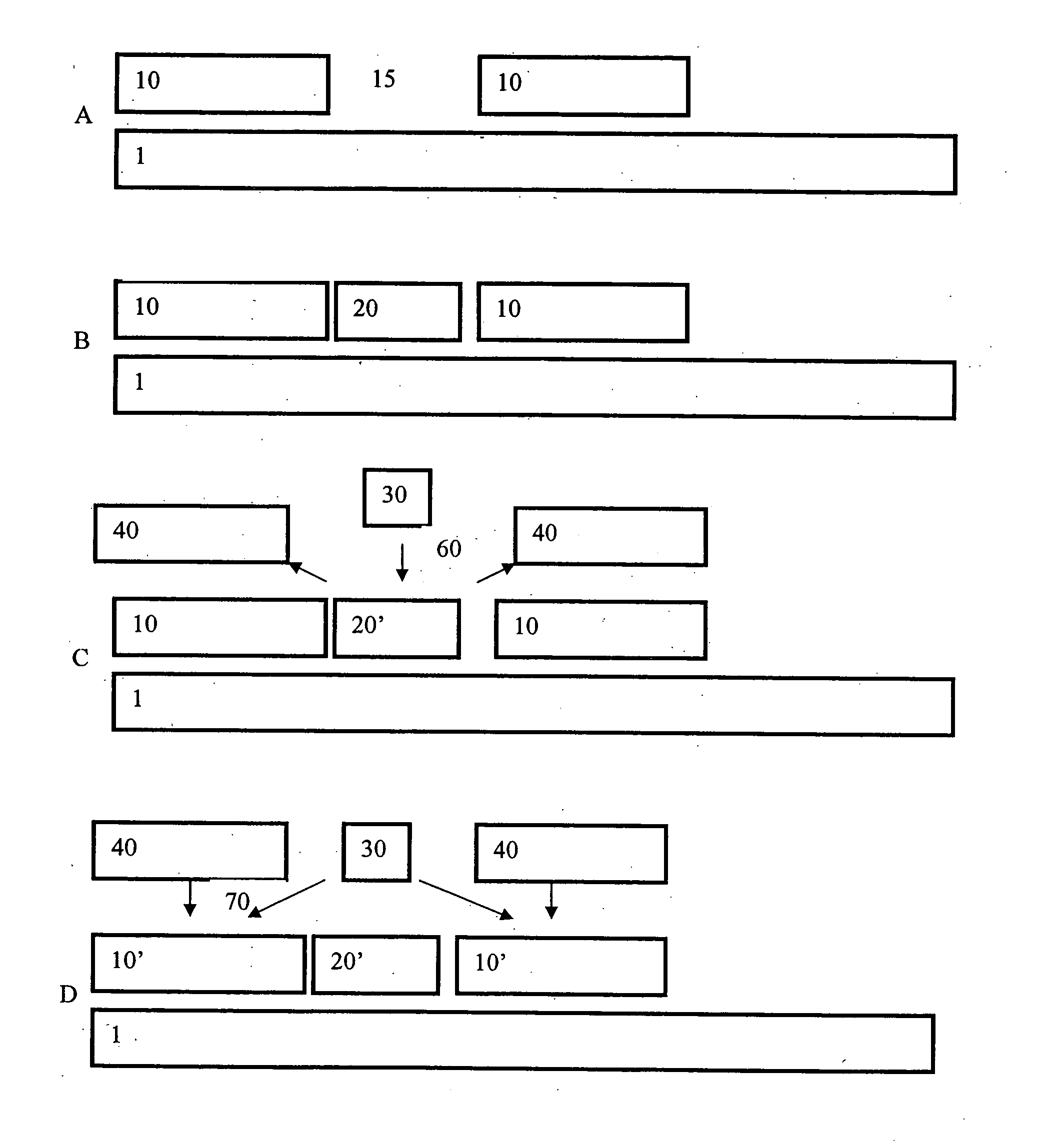
[0046] (a) La2O3 was deposited at 300° C. and below by ALD from La(thd)3 and O3 contains 10% carbon in the form of carbonate. A higher temperature of 350° C. is normally required to decompose the carbonate and remove nearly all the thd ligands to achieve pure La2O3 films. However, at reaction temperatures higher than 300° C., La(thd)3 starts decomposing, which results in non-uniform La2O3 thin films. Thus, while a higher temperature is desired in order to obtain a higher purity film, during the initial formation of the La(thd)3 monolayer, a lower temperature is desired to preserve uniformity of the initial monolayer. A catalytic reactant was used in this example to overcome this problem.
[0047] (b) At a temperature of 300° C. a La(thd)3 (primary reactant) pulse was introduced into a reaction chamber to contact a wafer on which La2O3 was to be deposited. Following this, excess primary reactant was removed from the chamber. Next, an Al(CH3)3 (catalytic reactant) pulse was introduced i...
example 2
[0048] First, a silicon compound such as gamma-aminopropyl triethoxy silane, hexamethyl disilazane or Si alkyl amide is pulsed into a reaction chamber to react with the surface of a wafer in a self-saturating manner. Next, unreacted silicon compound is removed from the chamber. After that, an Al compound such as Al(CH3)3 or Al(acac)3 is pulsed into the reaction chamber. Following this, excess Al compound is removed from the chamber. Following this, ozone is then pulsed into the reaction chamber. A thin film comprising a mixture of Al2O3 and SiO2 is obtained and the amount of Al2O3 incorporated into the film is controlled by the size of the Al compound (e.g., bigger ligands (e.g., Al(acac)3) results in less Al in the compound and smaller ligands (e.g., Al(CH3)3) results in more Al in compound). As discussed above, the size and number of the ligands can determine the amount of the catalytic reactant on the surface.
example 3
[0049] La(thd)3 is chemisorbed on a surface of a wafer at less than about 300° C. Excess La(thd)3 is removed from the reaction chamber. Following this Hacac or EtOH is pulsed into the reaction chamber and allowed to chemisorb to the surface. Next, excess Hacac or EtOH is removed from the chamber and O3 is pulsed into the chamber, resulting in deposition of an La2O3 / Al2O3 layer on the substrate. Finally, almost all O3 is removed from the chamber along with reaction byproducts, if any. The Hacac or EtOH allows a higher purity La2O3 / A2O3 monolayer to be produced than can be achieved by traditional ALD at this temperature, as these catalytic reactants only catalyze the full formation of an oxide of La(thd)3 and do not substantially contribute to the film.
PUM
| Property | Measurement | Unit |
|---|---|---|
| Temperature | aaaaa | aaaaa |
| Temperature | aaaaa | aaaaa |
| Time | aaaaa | aaaaa |
Abstract
Description
Claims
Application Information