

Semiconductor device manufacturing method, wafer and reticle
a semiconductor and manufacturing method technology, applied in semiconductor/solid-state device testing/measurement, instruments, photomechanical equipment, etc., can solve the problems of long measuring time, high cost, complicated measurement, etc., and achieve the effect of low cost and effective manufacturing of high-quality semiconductor devices
- Summary
- Abstract
- Description
- Claims
- Application Information
AI Technical Summary
Benefits of technology
Problems solved by technology
Method used
Image

Examples
Embodiment Construction
[0033] Preferred embodiments of the present invention will be described below with reference to the accompanying drawings, wherein like reference numerals refer to like elements throughout.
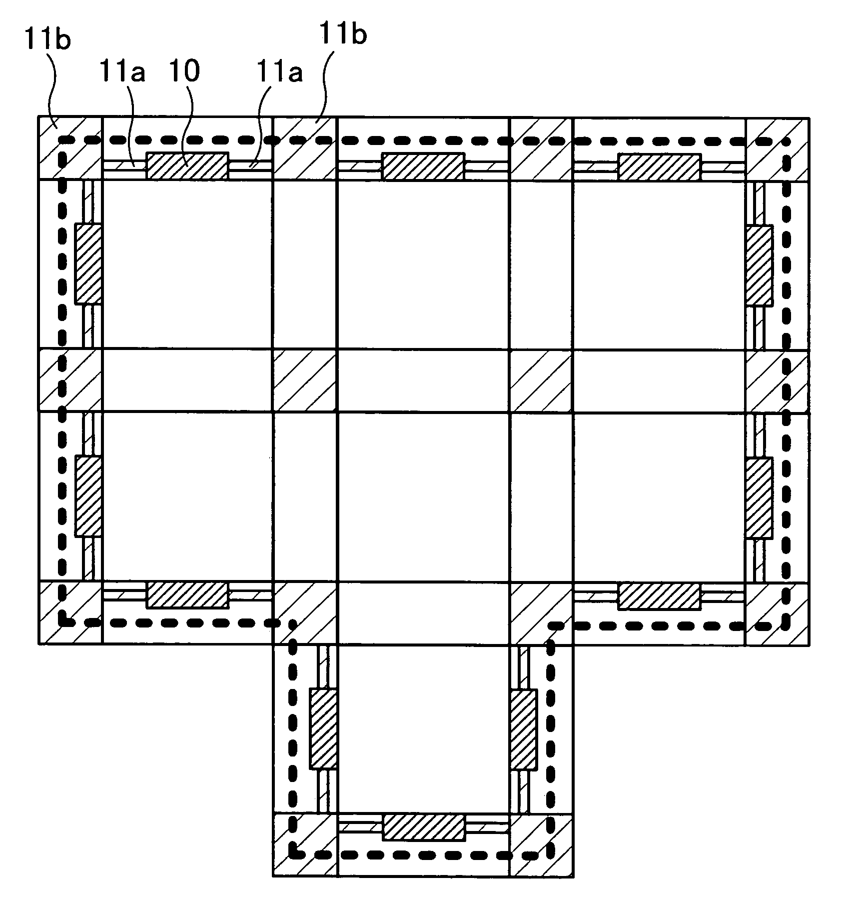
[0034]FIG. 2 shows a construction example of a reticle.
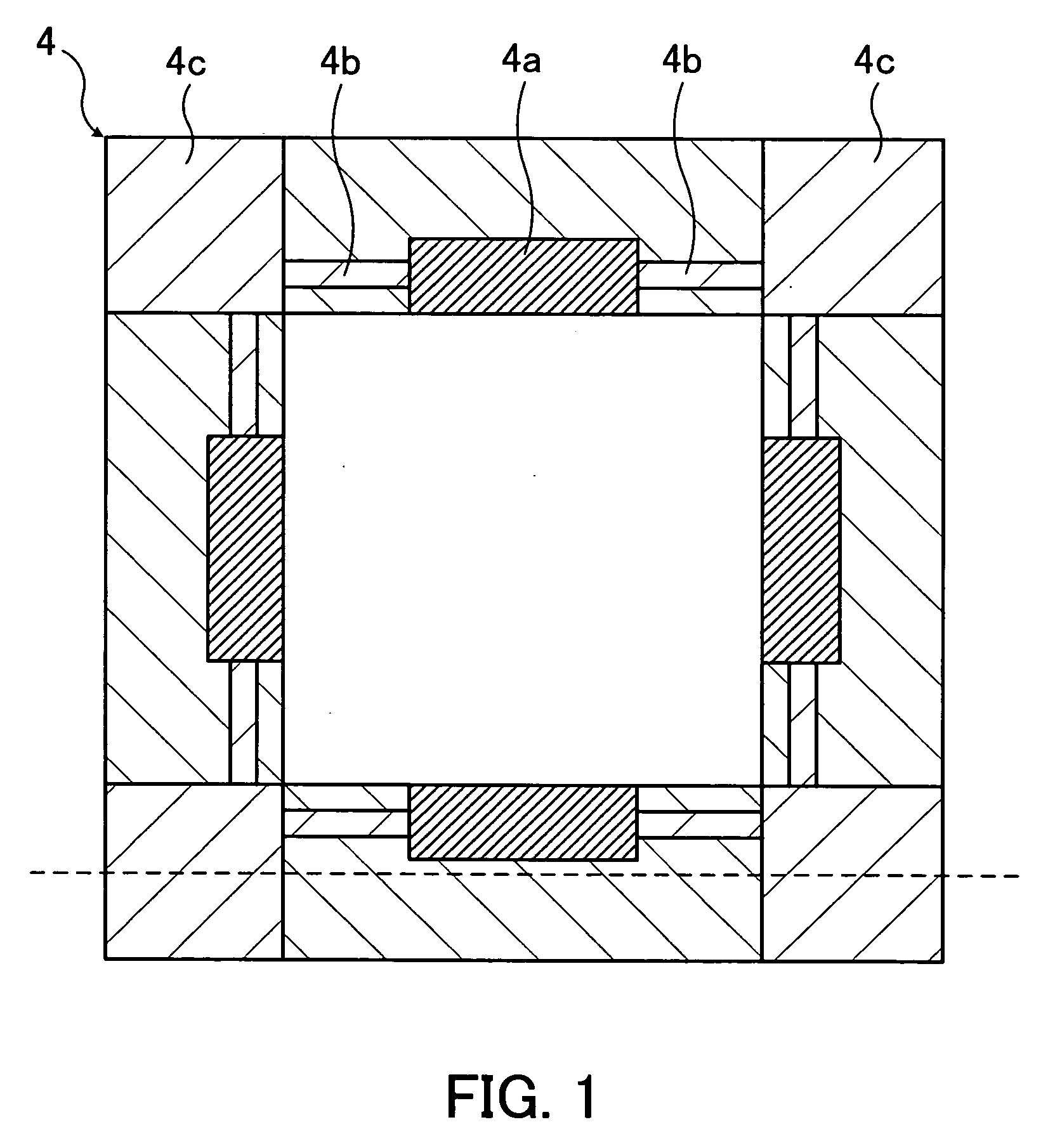
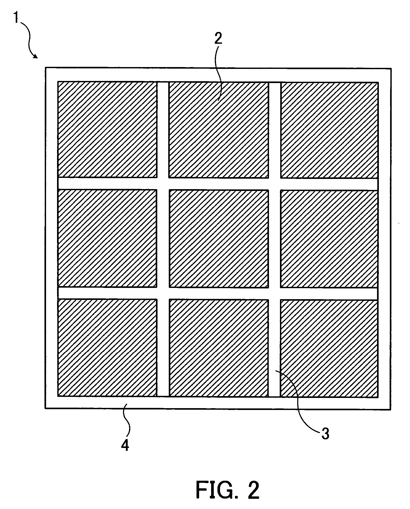
[0035] A reticle 1 exemplified in FIG. 2 has a total of 9 chip pattern formation areas (referred to as a “chip pattern area”) 2 arranged lengthwise 3 areas and widthwise 3 areas. The respective chip pattern areas 2 within the reticle 1 are zoned by a dicing area (referred to as an “inner dicing area”) 3 as a dicing line on a wafer. Further, in an outer periphery of the reticle 1, a dicing area (referred to as an “outer peripheral dicing area”) 4 is formed to surround the whole chip pattern area 2. When performing exposure of a plurality of shot positions using the reticle 1, the area 4 is served as the dicing line for dicing adjacent chips between different shot positions. When thus performing exposure of the plurality of shot positions, the...
PUM
 Abstract
Description
Claims
Application Information