Semiconductor-on-insulator type heterostructure and method of fabrication

Inactive Publication Date: 2007-03-08
S O I TEC SILICON ON INSULATOR THECHNOLOGIES
View PDF12 Cites 71 Cited by
  • Summary
  • Abstract
  • Description
  • Claims
  • Application Information

AI Technical Summary

Benefits of technology

[0031] The invention also relates to a semiconductor-on-insulator-type heterostructure comprising at least one insulating layer interposed between a receiver semiconductor substrate and an active semiconductor lay

Problems solved by technology

This improvement is achieved without recourse to the deposition of intermediate layers (i.e., amorphous or buffer layers), which previously would be deposited or interposed between t

Method used


Image

  • Semiconductor-on-insulator type heterostructure and method of fabrication
  • Semiconductor-on-insulator type heterostructure and method of fabrication
  • Semiconductor-on-insulator type heterostructure and method of fabrication

Examples


Example

Example 1

[0082] A donor substrate was prepared by growing a layer of germanium on silicon by epitaxy. Hydrogen and / or helium was then implanted in the germanium to create a zone of weakness. A silicon receiver substrate was also prepared by depositing therein an insulating layer of silicon oxide (SiO2) 250 nm to 300 nm thick.

[0083] Silicon was then implanted in the SiO2 layer to create therein a two-dimensional trapping layer. The implantation was carried out at an energy of 0.5 to 5 keV, at a dose of 5×10¹⁵ to 5×10¹⁶ Si+ ions / cm2. This resulted in formation of a layer of nanoparticles located between 1.5 nm and 4 nm (nanometers) beneath the surface of the SiO2 layer with a thickness in the range 2 nm to 3 nm.

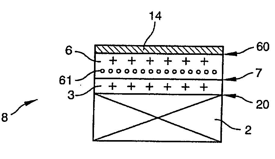
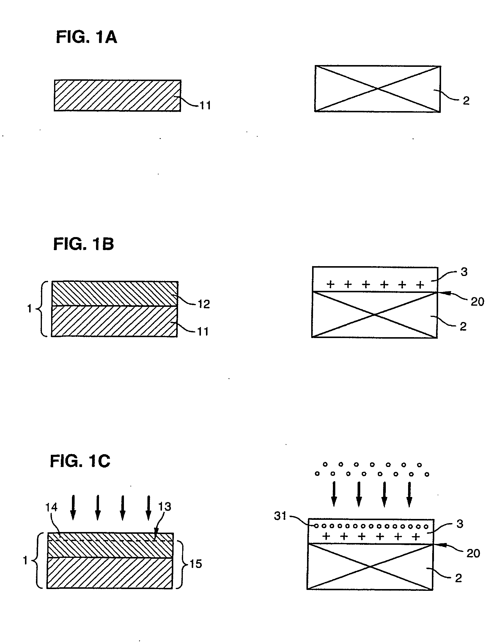
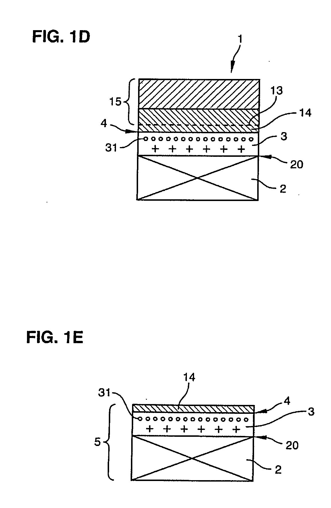
[0084] Bonding and detachment were carried out as described above with reference to FIGS. 1 and 2.

Example

Example 2

[0085]FIG. 4 is a drawing produced from a photograph obtained by transmission electron microscopy (TEM), and shows a trapping layer formed in a layer of SiO2 by implanting silicon at an energy of 1 keV and a dose of 1×10¹⁶ Si+ / cm2. The trapping layer 31 appears as a black line in the middle of the oxide 3.

[0086] In addition, tests were carried out to determine the range of energy and implantation dose to be used in producing the trapping layer when the insulator was made with silicon dioxide (SiO2) or silicon nitride (Si3N4).

[0087] When the insulator was silicon dioxide (SiO2), the implanted species preferably include silicon, germanium, or oxygen. In this case, either only one of the categories of atomic species mentioned below or several of them in succession may be implanted:

[0088] Silicon atoms with an implantation energy in the range 0.5 keV to 5 keV and an implantation dose in the range of 5×10¹⁵ to 5×10¹⁶ Si+ / cm2. Under these conditions, the layer of nanoparticle...


PUM


Abstract

The present invention relates to a method of fabricating a semiconductor-on-insulator-type heterostructure that includes at least one insulating layer interposed between a receiver substrate of semiconductor material and an active layer derived from a donor substrate of semiconductor material. The method includes the steps of bonding and active layer transfer. Prior to bonding, an atomic species which is identical or isoelectric with the insulating layer material is implanted in the insulating layer. The implantation forms a trapping layer, which can retain gaseous species present in the various interfaces of the heterostructure, thereby limiting formation of defects on the surface of the active layer.

Description

FIELD OF INVENTION [0001] The present invention relates to the field of semiconductors and, particularly, to fabrication of semiconductor-on-insulator-type heterostructures. BACKGROUND OF THE INVENTION [0002] A “semiconductor-on-insulator” (“SeOI”) type substrate is known. A SeOI type substrate generally comprises at least one insulating layer interposed between two layers of semiconductor material. A SeOI substrate or heterostructure has applications in many fields, especially in the fields of optics, electronics, and optoelectronics. [0003] SeOI substrates are generally fabricated using the following steps: [0004] forming or depositing an insulating layer on a first substrate termed the “donor” substrate, so that a “connection” interface exists between them; [0005] implanting atomic species within the donor substrate using a method known commercially as SMART-CUT® to form a zone of weakness therein; [0006] bonding a second substrate termed the “receiver” substrate onto the free su...

Claims


Application Information

Patent Timeline
IPC IPC(8): H01L21/30
CPCH01L21/76254Y10S438/974B82Y40/00H01L21/20
Inventor HEBRAS, XAVIER
Owner S O I TEC SILICON ON INSULATOR THECHNOLOGIES
Why Eureka
Try Eureka